Generic selectors
Exact matches only
Search in title
Search in content
Post Type Selectors

VD0685 Erbium(III) Oxide Evaporation Materials, Er2O3

Material Type: Erbium Oxide
Symbol: Er2O3
Color/Appearance: Pink, Solid
Purity: 99.9% ~ 99.99%
Shape: Powder/ Granule/ Custom-made

TFM is a prominent manufacturer and supplier of high-purity erbium(III) oxide evaporation materials, as well as a diverse range of other evaporation materials. We provide our products in both powder and granule forms, with custom options available to meet specific requirements.

Erbium(III) Oxide Evaporation Materials Overview

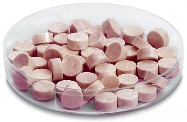
TFM specializes in high-purity erbium(III) oxide evaporation materials, with the chemical formula Er₂O₃. These materials are crucial for achieving superior film quality in various deposition processes. Our erbium(III) oxide evaporation materials are produced with up to 99.9995% purity, underscoring our commitment to quality and reliability.

Specifications

Material Type Erbium(III) Oxide
Form Evaporation Materials
Symbol Er2O3
Color/Appearance Pink Solid
Melting Point  2,344 °C
Density 8.64 g/cm3
Purity 99.5% ~ 99.99%
Shape Powder/ Granule/ Custom-made

Applications

Our erbium(III) oxide evaporation materials are versatile and used in various applications, including:

  • Deposition Processes: Suitable for semiconductor deposition, chemical vapor deposition (CVD), and physical vapor deposition (PVD).
  • Optical Applications: Ideal for wear-resistant coatings, decorative finishes, and display technologies.

Packaging and Handling

We ensure that our erbium(III) oxide evaporation materials are clearly tagged and labeled for easy identification and quality control. Careful handling during storage and transportation helps prevent any damage.

Contact Us

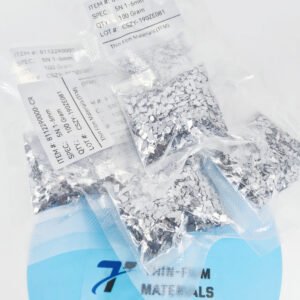
TFM is your trusted source for high-purity erbium(III) oxide evaporation materials. We offer these materials in several forms, including tablets, granules, rods, and wires. Custom shapes and quantities are available upon request. In addition, we provide evaporation sources, boats, filaments, crucibles, heaters, and e-beam crucible liners. For current pricing or to inquire about additional products, please contact us.

Reviews

There are no reviews yet.

Be the first to review “VD0685 Erbium(III) Oxide Evaporation Materials, Er2O3”

Your email address will not be published. Required fields are marked *

FAQ

  • They are high‐purity substances (e.g. metals, alloys, or compounds) used in thermal or electron‐beam evaporation processes to form thin films on substrates.

  • Typically, they’re processed into a form (often ingots, pellets, or wires) that can be efficiently vaporized. Preparation emphasizes high purity and controlled composition to ensure film quality.

  • Thermal evaporation and electron-beam (e-beam) evaporation are the two main techniques, where material is heated (or bombarded with electrons) until it vaporizes and then condenses on the substrate.

  • Thermal evaporation heats the material directly (often using a resistive heater), while e-beam evaporation uses a focused electron beam to locally heat and vaporize the source material—each method offering different control and energy efficiency.

  • Key parameters include source temperature, vacuum level, deposition rate, substrate temperature, and the distance between the source and the substrate. These factors influence film uniformity, adhesion, and microstructure.

  • Evaporation generally produces high-purity films with excellent control over thickness, and it is especially suitable for materials with relatively low melting points or high vapor pressures.

  • Challenges include issues with step coverage (due to line-of-sight deposition), shadowing effects on complex topographies, and possible re-evaporation of material from the substrate if temperature isn’t properly controlled.

  • Common evaporation materials include noble metals (e.g., gold, silver), semiconductors (e.g., silicon, germanium), metal oxides, and organic compounds—each chosen for its specific optical, electrical, or mechanical properties.

  • Selection depends on desired film properties (conductivity, optical transparency, adhesion), compatibility with the evaporation process, and the final device application (semiconductor, optical coating, etc.).

  • Optimizing substrate temperature, deposition rate, and chamber vacuum are critical for ensuring that the film adheres well and forms the intended microstructure without defects.

  • Troubleshooting may involve checking the source material’s purity, ensuring stable source temperature, verifying the vacuum level, adjusting the substrate’s position or temperature, and monitoring deposition rate fluctuations.

While evaporation tends to yield very high purity films with excellent thickness control, it is limited by its line-of-sight nature. In contrast, sputtering can deposit films more uniformly on complex surfaces and is more versatile for a broader range of materials.


Shopping Cart
Scroll to Top