Generic selectors
Exact matches only
Search in title
Search in content
Post Type Selectors

VD0709 Lead Zirconium Titanate Evaporation Materials, PbZr0.52Ti0.48O3

Catalog No.VD0709
MaterialLead Zirconium Titanate (PbZr0.52Ti0.48O3)
Purity99.9%
ShapePowder/ Granule/ Custom-made

Thin-Film Mat Engineering (TFM) is a leading provider of high-purity lead zirconium titanate (PZT) evaporation materials. We offer a wide range of evaporation materials in both powder and granule forms, with custom solutions available to meet specific needs. Our commitment to quality ensures that our materials deliver outstanding performance for various deposition applications.

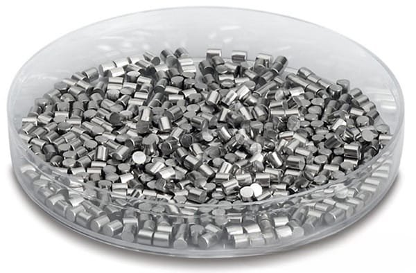
Lead Zirconium Titanate Evaporation Materials Overview

Thin-Film Mat Engineering (TFM) offers high-purity lead zirconium titanate (PZT) evaporation materials, with the chemical formula PbZr₀.₅₂Ti₀.₄₈O₃. These materials are vital for achieving superior quality films in various deposition processes. We ensure up to 99.9995% purity, supported by rigorous quality assurance methods to guarantee reliability.

Related Products: Lead Evaporation Materials, Zirconium Evaporation Materials, Titanium Evaporation Materials

Applications

Lead zirconium titanate evaporation materials are used in:

  • Deposition Processes: Ideal for semiconductor deposition, chemical vapor deposition (CVD), and physical vapor deposition (PVD).
  • Optics: Useful for wear protection, decorative coatings, and display technologies.

Packaging and Handling

Our lead zirconium titanate materials are carefully tagged and labeled to ensure effective identification and quality control. We take extensive measures to prevent any damage during storage and transportation.

Contact Us

At Thin-Film Mat Engineering (TFM), we provide high-purity lead zirconium titanate evaporation materials in various forms, including tablets, granules, rods, and wires. Customized shapes and quantities are available upon request. We also offer evaporation sources, boats, filaments, crucibles, heaters, and e-beam crucible liners. For current pricing and inquiries about additional materials, please contact us directly.

Reviews

There are no reviews yet.

Be the first to review “VD0709 Lead Zirconium Titanate Evaporation Materials, PbZr0.52Ti0.48O3”

Your email address will not be published. Required fields are marked *

FAQ

  • They are high‐purity substances (e.g. metals, alloys, or compounds) used in thermal or electron‐beam evaporation processes to form thin films on substrates.

  • Typically, they’re processed into a form (often ingots, pellets, or wires) that can be efficiently vaporized. Preparation emphasizes high purity and controlled composition to ensure film quality.

  • Thermal evaporation and electron-beam (e-beam) evaporation are the two main techniques, where material is heated (or bombarded with electrons) until it vaporizes and then condenses on the substrate.

  • Thermal evaporation heats the material directly (often using a resistive heater), while e-beam evaporation uses a focused electron beam to locally heat and vaporize the source material—each method offering different control and energy efficiency.

  • Key parameters include source temperature, vacuum level, deposition rate, substrate temperature, and the distance between the source and the substrate. These factors influence film uniformity, adhesion, and microstructure.

  • Evaporation generally produces high-purity films with excellent control over thickness, and it is especially suitable for materials with relatively low melting points or high vapor pressures.

  • Challenges include issues with step coverage (due to line-of-sight deposition), shadowing effects on complex topographies, and possible re-evaporation of material from the substrate if temperature isn’t properly controlled.

  • Common evaporation materials include noble metals (e.g., gold, silver), semiconductors (e.g., silicon, germanium), metal oxides, and organic compounds—each chosen for its specific optical, electrical, or mechanical properties.

  • Selection depends on desired film properties (conductivity, optical transparency, adhesion), compatibility with the evaporation process, and the final device application (semiconductor, optical coating, etc.).

  • Optimizing substrate temperature, deposition rate, and chamber vacuum are critical for ensuring that the film adheres well and forms the intended microstructure without defects.

  • Troubleshooting may involve checking the source material’s purity, ensuring stable source temperature, verifying the vacuum level, adjusting the substrate’s position or temperature, and monitoring deposition rate fluctuations.

While evaporation tends to yield very high purity films with excellent thickness control, it is limited by its line-of-sight nature. In contrast, sputtering can deposit films more uniformly on complex surfaces and is more versatile for a broader range of materials.


Shopping Cart
Scroll to Top