Generic selectors
Exact matches only
Search in title
Search in content
Post Type Selectors

VD0759 Zirconium Nitride Evaporation Materials, ZrN

Catalog No.VD0759
MaterialZirconium Nitride (ZrN)
Purity99.5%
ShapePowder/ Granule/ Custom-made
TFM is a premier manufacturer and supplier of high-purity Zirconium Nitride (ZrN) evaporation materials. We provide these materials in both powder and granule forms, catering to various deposition needs. Custom shapes and quantities are also available upon request to suit specific applications. Our dedication to quality ensures that our evaporation materials meet the highest standards.

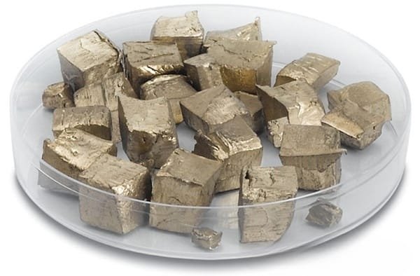
Zirconium Nitride Evaporation Materials Overview

TFM provides high-purity Zirconium Nitride (ZrN) evaporation materials, essential for creating high-quality thin films in various deposition processes. With the chemical formula ZrN, our materials are known for their exceptional purity, reaching up to 99.9995% due to our rigorous quality assurance methods.

Related Products

Zirconium Nitride Evaporation Materials Specification

Material TypeZirconium Nitride
SymbolZrN
Appearance/ColorYellow-brown solid
Melting Point2,952 °C (5,346 °F; 3,225 K) at 760 mmHg
Density7.09 g/cm3 (24 °C)
Purity99.5%
ShapePowder/ Granule/ Custom-made

Applications of Zirconium Nitride Evaporation Materials

Zirconium Nitride evaporation materials are utilized in:

  • Deposition Processes: Crucial for semiconductor deposition, chemical vapor deposition (CVD), and physical vapor deposition (PVD).
  • Optics: Ideal for wear protection, decorative coatings, and display technologies.

Packaging and Handling

Our Zirconium Nitride evaporation materials are carefully tagged and labeled to facilitate efficient identification and quality control. We ensure that packaging is robust to prevent any damage during storage and transportation.

Contact Information

TFM is a leading supplier of high-purity Zirconium Nitride evaporation materials, available in various forms such as tablets, granules, rods, and wires. Customized shapes and quantities can be requested. We also offer evaporation sources, boats, filaments, crucibles, heaters, and e-beam crucible liners. For current pricing and inquiries about other materials, please contact us directly.

Reviews

There are no reviews yet.

Be the first to review “VD0759 Zirconium Nitride Evaporation Materials, ZrN”

Your email address will not be published. Required fields are marked *

FAQ

  • They are high‐purity substances (e.g. metals, alloys, or compounds) used in thermal or electron‐beam evaporation processes to form thin films on substrates.

  • Typically, they’re processed into a form (often ingots, pellets, or wires) that can be efficiently vaporized. Preparation emphasizes high purity and controlled composition to ensure film quality.

  • Thermal evaporation and electron-beam (e-beam) evaporation are the two main techniques, where material is heated (or bombarded with electrons) until it vaporizes and then condenses on the substrate.

  • Thermal evaporation heats the material directly (often using a resistive heater), while e-beam evaporation uses a focused electron beam to locally heat and vaporize the source material—each method offering different control and energy efficiency.

  • Key parameters include source temperature, vacuum level, deposition rate, substrate temperature, and the distance between the source and the substrate. These factors influence film uniformity, adhesion, and microstructure.

  • Evaporation generally produces high-purity films with excellent control over thickness, and it is especially suitable for materials with relatively low melting points or high vapor pressures.

  • Challenges include issues with step coverage (due to line-of-sight deposition), shadowing effects on complex topographies, and possible re-evaporation of material from the substrate if temperature isn’t properly controlled.

  • Common evaporation materials include noble metals (e.g., gold, silver), semiconductors (e.g., silicon, germanium), metal oxides, and organic compounds—each chosen for its specific optical, electrical, or mechanical properties.

  • Selection depends on desired film properties (conductivity, optical transparency, adhesion), compatibility with the evaporation process, and the final device application (semiconductor, optical coating, etc.).

  • Optimizing substrate temperature, deposition rate, and chamber vacuum are critical for ensuring that the film adheres well and forms the intended microstructure without defects.

  • Troubleshooting may involve checking the source material’s purity, ensuring stable source temperature, verifying the vacuum level, adjusting the substrate’s position or temperature, and monitoring deposition rate fluctuations.

While evaporation tends to yield very high purity films with excellent thickness control, it is limited by its line-of-sight nature. In contrast, sputtering can deposit films more uniformly on complex surfaces and is more versatile for a broader range of materials.


Shopping Cart
Scroll to Top