Introduction
Nickel Silicide Evaporation Materials (NiSi₂) are advanced compound materials used in thin film deposition for semiconductor and microelectronic applications. Nickel silicides are widely recognized for their excellent electrical conductivity, low resistivity, and strong compatibility with silicon-based devices, making them essential materials in modern integrated circuit fabrication.
When deposited through thermal evaporation or electron beam evaporation, NiSi₂ materials form thin films that are frequently used as contact layers, diffusion barriers, and interconnect materials in semiconductor structures. Their ability to create stable interfaces with silicon substrates makes nickel silicide an important material in advanced microelectronic manufacturing.
Detailed Description
Nickel Silicide evaporation materials are typically produced from high-purity nickel and silicon through controlled alloying and compound synthesis processes. Advanced manufacturing techniques such as vacuum melting, powder metallurgy, or sintering are used to achieve a homogeneous material structure with consistent stoichiometry.
Among various nickel silicide phases, NiSi₂ is particularly attractive for semiconductor applications because of its relatively low electrical resistivity and excellent thermal stability. It forms a well-defined interface with silicon substrates, enabling reliable electrical contacts in integrated circuits.
Nickel silicide films are commonly used in self-aligned silicide (salicide) processes, where nickel reacts with silicon to form a conductive silicide layer on transistor source and drain regions. This reduces contact resistance and improves device performance.
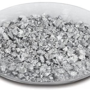
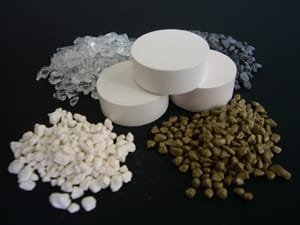
In evaporation deposition systems, NiSi₂ materials can be supplied in forms such as pellets, granules, tablets, or pieces, compatible with tungsten boats, crucibles, or electron beam evaporation sources. High-purity materials ensure stable evaporation behavior and consistent thin film composition.
Applications
Nickel Silicide evaporation materials are widely used in semiconductor and electronic technologies:
Semiconductor device fabrication, particularly contact and interconnect layers
Self-aligned silicide (salicide) processes in integrated circuits
Low-resistance contact formation for silicon devices
Microelectronic thin film deposition
Advanced electronic materials research
Thin film metallization layers in silicon-based electronics
Technical Parameters
| Parameter | Typical Value / Range | Importance |
|---|---|---|
| Chemical Formula | NiSi₂ | Determines compound stoichiometry |
| Purity | 99.9% – 99.99% | Ensures stable electrical properties |
| Form | Pellets / Granules / Tablets / Pieces | Compatible with evaporation systems |
| Particle Size | 1 – 6 mm typical | Supports uniform evaporation |
| Deposition Method | Thermal evaporation / E-beam evaporation | Suitable for PVD thin film processes |
| Density | High-density compound material | Ensures stable evaporation behavior |
Comparison with Related Materials
| Material | Key Advantage | Typical Application |
|---|---|---|
| Nickel Silicide (NiSi₂) | Low resistivity and strong silicon compatibility | Semiconductor contacts and interconnects |
| Nickel (Ni) | High conductivity and good adhesion | Metallization layers |
| Titanium Silicide (TiSi₂) | Very low resistivity for high-speed devices | Semiconductor contacts |
FAQ
| Question | Answer |
|---|---|
| What deposition methods are suitable for NiSi₂ evaporation materials? | NiSi₂ materials are commonly used in thermal evaporation and electron beam evaporation systems. |
| What forms are available for evaporation materials? | Typical forms include pellets, granules, tablets, rods, or custom pieces. |
| Why is nickel silicide used in semiconductor devices? | Nickel silicide provides low-resistance electrical contacts and excellent compatibility with silicon. |
| Can the material composition be customized? | Yes. Different nickel silicide phases or compositions can be produced depending on application requirements. |
| What substrates can NiSi₂ films be deposited on? | NiSi₂ films are commonly deposited on silicon wafers and other semiconductor substrates. |
Packaging
Our Nickel Silicide Evaporation Materials (NiSi₂) are meticulously tagged and labeled externally to ensure efficient identification and maintain strict quality control standards. The materials are packaged in vacuum-sealed or inert atmosphere containers to prevent oxidation and contamination. Protective cushioning and export-grade cartons or wooden crates ensure safe transportation and storage.
Conclusion
Nickel Silicide Evaporation Materials (NiSi₂) provide a reliable solution for depositing conductive thin films used in semiconductor device fabrication and microelectronics. Their excellent compatibility with silicon, low resistivity, and stable thermal properties make them ideal for forming high-performance contact layers and interconnect structures.
With high purity, customizable forms, and stable evaporation performance, NiSi₂ evaporation materials are well suited for advanced semiconductor manufacturing and research applications.
For detailed specifications and a quotation, please contact us at sales@thinfilmmaterials.com.


 MSDS File


Reviews
There are no reviews yet.