 MSDS File
Introduction
Lead(II) Sulfide (PbS) Evaporation Materials are widely used in vacuum thin-film deposition for infrared (IR) optoelectronic and semiconductor applications. As a narrow-bandgap semiconductor, PbS exhibits strong infrared absorption and tunable electrical properties, making it a key material for IR detectors, photoconductive devices, and advanced sensor research.
Detailed Description
Our Lead(II) Sulfide Evaporation Materials are produced from high-purity lead and sulfur using carefully controlled synthesis processes to ensure accurate stoichiometry and phase consistency. For PbS-based thin films, maintaining the correct Pb:S ratio is critical, as even small deviations can significantly affect carrier concentration, optical absorption, and film stability.
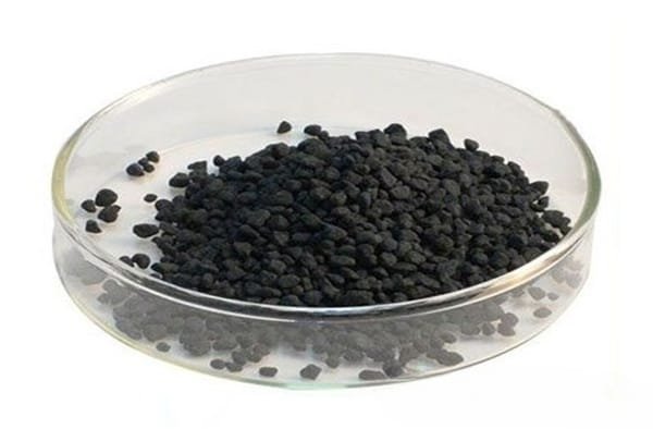
The material is supplied in evaporation-ready forms such as pellets, pieces, or granules, suitable for thermal evaporation and electron-beam evaporation systems. Optimized particle size and density promote smooth, stable evaporation behavior, reducing spitting, compositional drift, and particle contamination during deposition. High material purity helps achieve dense, uniform films with reproducible optoelectronic performance.
PbS evaporation materials are compatible with high-vacuum (HV) and ultra-high-vacuum (UHV) environments and are commonly used in single-source evaporation for compound film formation. Custom material forms, purity grades, and batch sizes are available to support both laboratory-scale research and industrial coating processes.
Applications
Lead(II) Sulfide Evaporation Materials are commonly used in:
Infrared (IR) detectors and photoconductive sensors
Semiconductor and optoelectronic thin films
Thermal imaging and IR spectroscopy components
Research on narrow-bandgap semiconductor materials
Academic and industrial R&D laboratories
They are particularly suitable for applications requiring strong IR sensitivity and controlled semiconductor behavior.
Technical Parameters
| Parameter | Typical Value / Range | Importance |
|---|---|---|
| Chemical Formula | PbS | Defines narrow-bandgap semiconductor properties |
| Purity | 99.9% – 99.99% | Reduces impurities affecting optical and electrical performance |
| Form | Pellets / Pieces / Granules | Compatible with different evaporation sources |
| Deposition Method | Thermal / E-beam evaporation | Supports standard vacuum deposition techniques |
| Vacuum Compatibility | HV / UHV | Ensures clean film growth |
| Packaging | Vacuum-sealed | Prevents oxidation and contamination |
Comparison with Related Materials
| Material | Key Advantage | Typical Application |
|---|---|---|
| Lead(II) Sulfide (PbS) | Strong IR absorption, narrow bandgap | IR detectors and sensors |
| Lead Selenide (PbSe) | Longer IR wavelength response | Advanced IR optoelectronics |
| Cadmium Sulfide (CdS) | Wider bandgap | Visible-range optoelectronics |
FAQ
| Question | Answer |
|---|---|
| Is PbS suitable for e-beam evaporation? | Yes, PbS can be deposited using both thermal and e-beam evaporation methods. |
| Can material form be customized? | Yes, pellets, chunks, and granules can be tailored to your evaporation source. |
| How is stoichiometry ensured? | Controlled synthesis and batch inspection ensure consistent PbS composition. |
| Are small R&D quantities available? | Yes, we support both small research orders and bulk supply. |
Packaging
Our Lead(II) Sulfide Evaporation Materials are vacuum-sealed, clearly labeled, and securely packaged to maintain purity and prevent contamination during storage and transportation.
Conclusion
Lead(II) Sulfide (PbS) Evaporation Materials provide a reliable and high-purity source for depositing infrared-sensitive semiconductor thin films. With controlled stoichiometry, flexible material forms, and compatibility with standard vacuum evaporation techniques, they are well suited for both research and industrial IR applications.
For detailed specifications and a quotation, please contact us at sales@thinfilmmaterials.com.


Reviews
There are no reviews yet.