Introduction to Deposition Materials
Deposition Materials play a fundamental role in numerous industries, such as electronics, optics, and manufacturing, by facilitating the creation of functional films and coatings. These materials are essential for a wide array of applications ranging from semiconductor devices to optical coatings, providing enhanced surface properties and improving product performance. The process of applying these materials typically involves various thin film deposition techniques, which are designed to deposit thin films onto substrates with high precision and control.
At the core of thin film deposition are two primary categories: physical deposition and chemical deposition. Physical vapour deposition (PVD), which encompasses methods such as sputtering and evaporation, involves the physical transfer of deposition materials from a source to a substrate. In contrast, chemical vapour deposition (CVD) relies on chemical reactions to form thin films, a process exemplified by plasma enhanced chemical vapour deposition, which increases deposition rates and enhances film quality at lower temperatures.
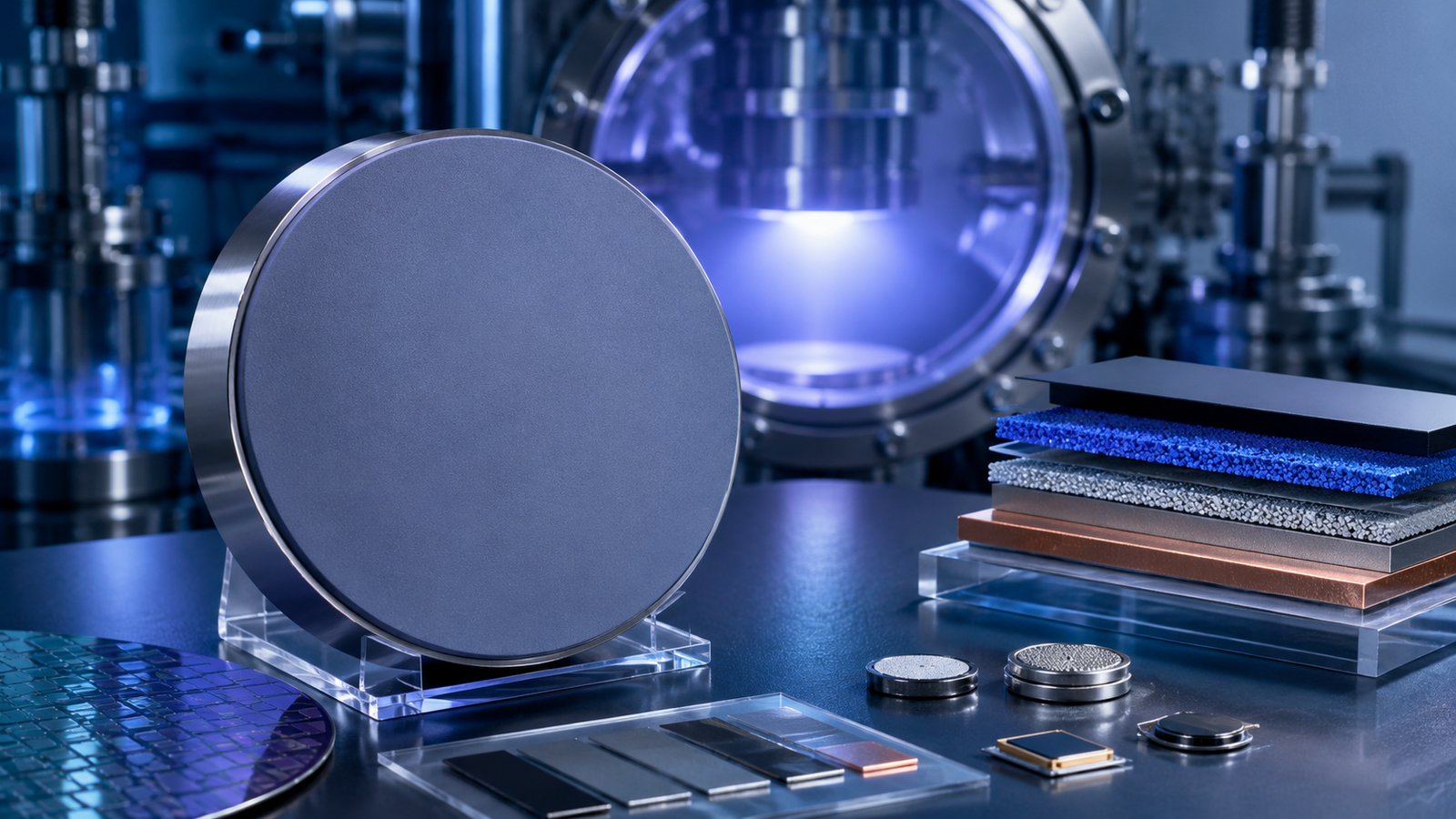
The effectiveness of these processes is heavily dependent on the types of deposition materials utilized. Specific materials, such as Sputtering Targets and Evaporation Materials, are selected based on desired properties like conductivity, thickness, and adherence. Similarly, the choice of evaporation sources, including different types of Crucibles or evaporation techniques, directly impacts the quality of thin film coatings. As technological advancements continue to evolve, the demand for high-performance deposition materials has become increasingly significant, particularly for applications like chemical vapor deposition graphene, which holds promise for next-generation electronic devices.
In addition, the continuous development in deposition technology has led to an expansive array of materials tailored for specific applications. This creativity and adaptability illustrate the critical nature of deposition materials in fulfilling the precise requirements of modern manufacturing processes. The significance of these materials cannot be overstated, as they play an indispensable role in shaping the future of technology.
Types of Deposition Materials
Deposition materials can be categorized into two primary types: organic and inorganic materials. Each category encompasses various substances with distinct characteristics, which provide specific advantages and limitations based on their intended applications. Understanding the differences between these materials is crucial for selecting the appropriate deposition techniques such as physical vapour deposition, chemical vapor deposition graphene, and others.
Organic deposition materials include polymers and organic compounds. Polymers, such as polyimides and polyethylene, are often utilized in thin film coatings due to their flexibility and insulation properties. They can be deposited through various thin film deposition techniques, including spin coating and screen printing. The advantage of organic materials lies in their excellent mechanical properties and the ability to create large-area films. However, they typically exhibit lower thermal and chemical stability compared to inorganic materials, limiting their use in high-temperature environments.
In contrast, inorganic deposition materials primarily consist of metals, ceramics, and semiconductors. Metals such as Aluminum, Copper, and Gold are frequently used as deposition materials in the manufacturing of electronic components and microelectronics. They can be applied through processes such as sputtering and thermal evaporation, where evaporation sources like crucibles and vacuum furnaces facilitate the deposition process. Ceramics, which include materials like silicon carbide and aluminum oxide, boast high hardness and thermal stability, making them ideal for wear-resistant applications. However, the brittleness of ceramics can pose challenges in certain manufacturing processes.
Both organic and inorganic materials play significant roles in thin film deposition techniques, and the choice between them depends on factors such as application requirements, desired properties, and environmental conditions. Understanding the unique characteristics and limitations of each type of deposition material enables researchers and manufacturers to innovate and optimize their processes effectively.
Popular Product Types in Deposition Technology
Deposition materials play a critical role in various manufacturing processes, particularly in the production of thin film materials used in electronic components and coatings. Among the most commonly used materials are sputtering targets, evaporation materials, and chemical vapor deposition (CVD) precursors. Each of these materials contributes significantly to the characteristics of the final product.
Sputtering Targets are essential in physical vapor deposition (PVD) techniques. These targets are typically made from metals, ceramics, or compound materials that are sputtered off onto a substrate during the deposition process. The attributes of sputtering targets, such as purity and composition, directly affect the quality of the thin film coatings produced. High-purity sputtering targets are crucial for applications in integrated circuits and optical coatings, where precision is paramount.
Evaporation Materials, another key family of deposition materials, are heated in vacuum environments to produce vapor, which subsequently condenses into thin films on substrates. Common evaporation sources include various metals like gold, aluminum, and alloys. The choice of evaporation materials is pivotal as it impacts not only the thickness and uniformity of thin film deposition but also the material’s physical properties, such as electrical and thermal conductivity.
Chemical vapor deposition (CVD) involves the use of gaseous precursors that react chemically to form thin films. The definition of chemical deposition underscores its importance in creating materials such as graphene, which has a wide range of applications from electronics to advanced coatings. Plasma enhanced chemical vapor deposition (PECVD) is a variation that utilizes plasma to enhance the reaction rates, allowing for the deposition of materials at lower temperatures and contributing to improved film properties.
In conclusion, understanding the various deposition materials, including sputtering targets, evaporation sources, and CVD precursors, is crucial for optimizing thin film deposition techniques. The selection of appropriate materials directly influences the performance and application of the resulting thin films in a variety of technologies.
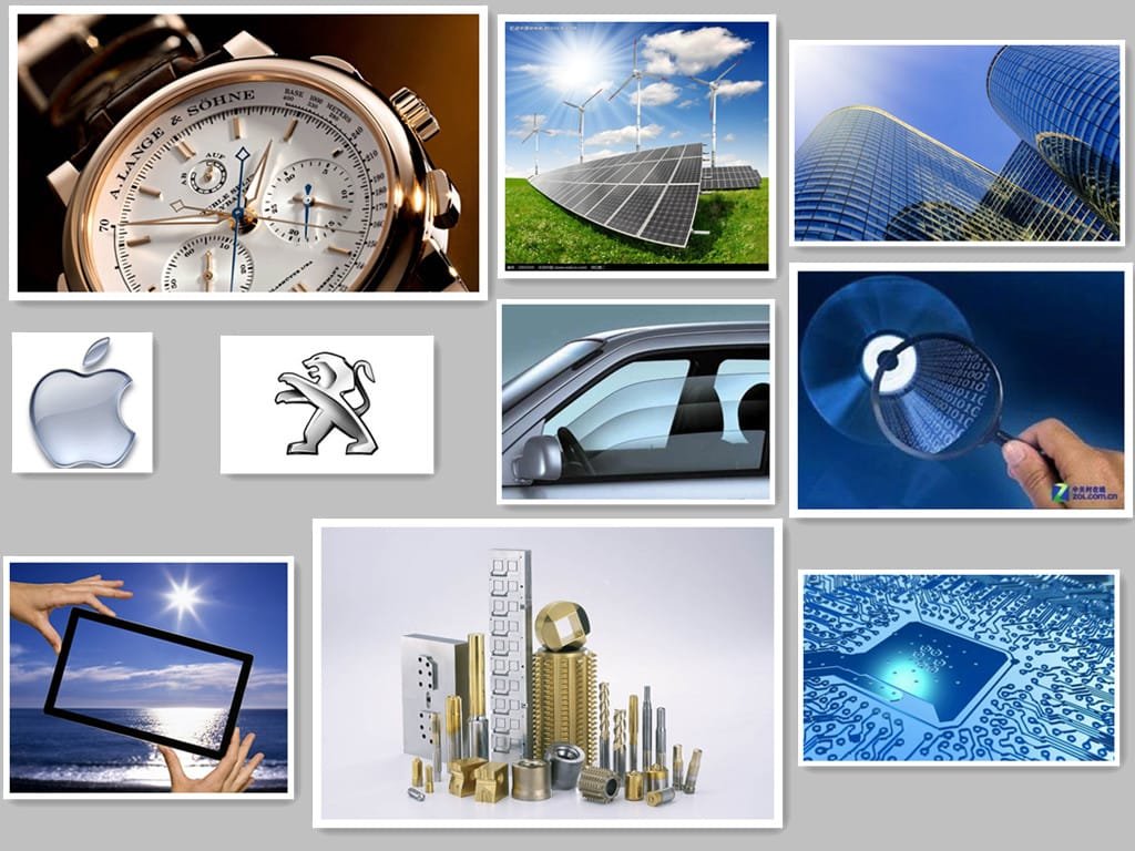
Applications of Deposition Materials
Deposition materials play a critical role across various industries, enabling the production of advanced thin films and coatings with specific properties tailored to meet the demands of modern technology.
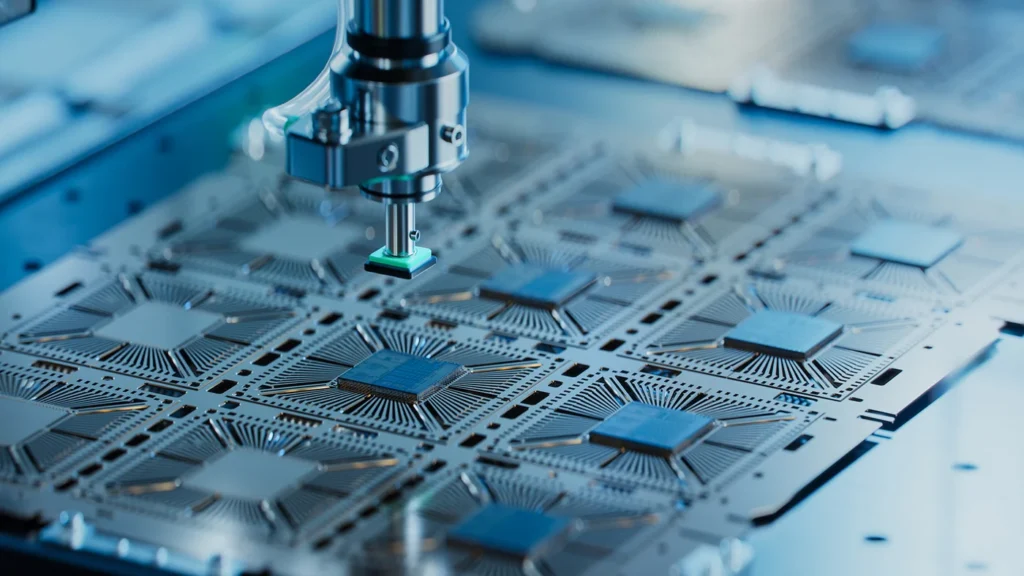
One significant application is in semiconductor manufacturing, where thin film deposition techniques such as chemical vapor deposition (CVD) and physical vapor deposition (PVD) are utilized to create the intricate layers found in microelectronic devices. For instance, in producing integrated circuits, deposition materials like silicon and silicon dioxide are essential for forming the gate oxides and conducting layers that are crucial to device functionality.
Another important application lies in the realm of optical coatings, where deposition materials are employed to enhance the performance of lenses and mirrors. Thin film coatings produced using techniques like sputtering or evaporation can dramatically improve reflectivity, transmissivity, and durability. Advanced optical applications, such as anti-reflective coatings for eyeglasses or high-reflectivity coatings for lasers, showcase how innovative material selection and deposition processes have led to enhanced visual acuity and energy efficiency.

Surface protection is a further area where deposition materials find significant use. In industries such as aerospace, automotive, and medical, thin films generated through techniques like plasma-enhanced chemical vapor deposition (PECVD) can create highly durable, corrosion-resistant coatings. These coatings help extend the lifespan of components and ensure reliability in demanding environments. For example, titanium and its alloys can be coated with hard ceramic materials to improve wear resistance and surface hardness.

The versatility of deposition materials extends to applications in solar energy technology as well. Thin films used in photovoltaic cells are typically produced via vacuum processing techniques, which can include both physical and chemical deposition methods. Materials like cadmium telluride or amorphous silicon are increasingly being integrated to enhance energy conversion efficiency and reduce production costs.
Key Deposition Technologies
Deposition technologies are essential methods utilized to create thin film coatings across various industries. Among the most prominent techniques are Physical Vapor Deposition (PVD), Chemical Vapor Deposition (CVD), and Atomic Layer Deposition (ALD). Each method operates on unique principles and offers specific advantages in producing deposition materials.
Physical Vapor Deposition (PVD) encompasses processes such as sputtering and thermal evaporation, where solid materials are vaporized in a vacuum and subsequently deposited onto a substrate. Sputtering targets are commonly used, where energetic particles cause the material to eject atoms. This technique is widely adopted for its ability to produce durable coatings suitable for applications in electronics, optics, and tool manufacturing. PVD is particularly valued for its ability to create adhesion and improved mechanical properties in thin film materials.
On the other hand, Chemical Vapor Deposition (CVD) refers to techniques involving chemical reactions to produce thin films. In this process, gaseous precursors react at elevated temperatures to form a solid material that deposits on a substrate. Variants like Plasma Enhanced Chemical Vapor Deposition (PECVD) enhance the process by using plasma to lower the reaction temperature, which is beneficial for sensitive substrates. CVD is particularly favored for producing high-purity materials and is extensively used in the semiconductor industry for applications such as chemical vapor deposition graphene.
Another noteworthy method is Atomic Layer Deposition (ALD), which manages to deposit material layer by layer, ensuring precise control over thickness. This technique is highly efficient for creating uniform coatings over complex geometries and is increasingly utilized in fields such as nanotechnology and energy storage. In comparison, both CVD and ALD demonstrate superiority in uniformity and conformality, while PVD stands out for simplicity and speed. Understanding these thin film deposition techniques aids in selecting the most suitable method for specific applications across industries.
Material Selection Criteria
When selecting deposition materials for thin film deposition techniques, several critical criteria must be taken into account to ensure optimal performance and compatibility with specific applications. The choice of materials can significantly impact the efficiency, durability, and overall functionality of the resulting thin film coatings.
*One of the foremost considerations is substrate compatibility. The deposition materials must adhere effectively to the substrate to provide a robust bond, which involves examining the surface energy, roughness, and chemical properties of the substrate in relation to the chosen material.
*Thermal stability is another vital factor in the selection process. Many deposition processes, such as physical vapor deposition and chemical vapor deposition, involve elevated temperatures. Thus, the thermal properties of the deposition materials must align with the operating conditions of the coating technique. Materials that cannot withstand high temperatures may lead to unexpected reactions, compromising the integrity of the thin films produced.
*Environmental resistance also plays a crucial role in material selection. Depending on the intended application, the deposition materials must exhibit adequate resistance to environmental factors such as humidity, temperature fluctuations, and exposure to chemicals. Those designed for high-stress environments, for instance, may require specific coatings or treatments to enhance corrosion or wear resistance.
*Lastly, the purpose of the coating significantly influences the choice of deposition materials. For applications in electronics, materials such as graphene may be preferred for their excellent electrical conductivity, while optical coatings often require specific thin film materials that optimize light transmission.
By carefully considering these criteria—substrate compatibility, thermal stability, environmental resistance, and coating purpose—users can make informed decisions regarding the appropriate deposition materials for their specific applications. This thoughtful approach ensures the production of high-quality, functional thin films that meet the desired specifications.
Challenges in the Use of Deposition Materials
The utilization of deposition materials in various sectors presents several challenges that can significantly impact the effectiveness and quality of the resulting thin film coatings.
One prominent issue is material degradation during the deposition process. As deposition techniques, such as physical vapor deposition (PVD) and chemical vapor deposition (CVD), are employed, exposure to high temperatures, reactive environments, and other harsh conditions may lead to the deterioration of the film’s properties. This degradation can ultimately result in compromised performance and longevity of the thin films, particularly when employing sensitive evaporation materials and sputtering targets.
Another critical challenge lies in adhesion issues. Successful thin film deposition relies heavily on the ability of films to adhere adequately to substrate materials. Inadequate adhesion can lead to delamination, which undermines the integrity of coatings applied on substrates used, for instance, in electronic devices or optical components. Various factors affect adhesion, including surface preparation and the intrinsic properties of both the substrate and the deposition materials. Research into innovative thin film deposition techniques, such as plasma enhanced chemical vapor deposition (PECVD), aims to enhance adhesion through the activation of surface chemistry or modifications in film growth processes.
Environmental constraints also pose significant challenges in the deposition process. Compliance with environmental regulations impacts the choice of materials and processes used in thin film fabrication. For example, certain chemical vapor deposition graphene methods may generate volatile organic compounds that need to be managed to reduce environmental impact. Consequently, researchers are exploring sustainable alternatives and advancements in deposition technologies that minimize ecological footprints while maximizing material performance.
By addressing these challenges through ongoing research and technological innovations, the effectiveness of deposition materials can be improved, facilitating their broader application and enhancing the performance of thin films across industries.
Future Trends in Deposition Materials and Technologies
The landscape of deposition materials is rapidly evolving, driven by technological advancements and the increasing demand for sustainable and efficient solutions across various industries. One of the most significant trends is the rise of eco-friendly materials. Manufacturers are exploring deposition methods that minimize environmental impact while maintaining performance. This includes the development of biodegradable thin film materials and alternative chemical vapor deposition techniques that utilize less harmful substances, aligning with global sustainability goals.
Advancements in nanotechnology also play a crucial role in shaping the future of deposition materials. Nanostructured thin film coatings are becoming integral in applications ranging from electronics to healthcare. Techniques such as physical vapor deposition (PVD) are being optimized to apply nanoscale layers, leading to enhanced properties such as improved thermal and electrical conductivity. Additionally, the integration of nanomaterials in chemical vapor deposition processes, including plasma enhanced chemical vapor deposition (PECVD), offers the potential for innovative functional coatings that can interact with their environment in unprecedented ways.
Composite materials are increasingly being researched and employed within deposition technologies, contributing to lighter yet stronger components in sectors such as aerospace and automotive. Innovations in thin film deposition techniques are enabling the fabrication of multi-layer structures that can combine various material properties for enhanced performance. Sputtering targets and evaporation materials are being refined to ensure precise control over layer composition and thickness, resulting in functional coatings that meet the specific requirements of advanced applications.
As industries continue to evolve, the demand for tailored deposition materials and techniques will grow. Improved vacuum furnaces and filaments are being developed, making the deposition processes more efficient and controllable. The convergence of these trends heralds a new era for deposition technologies, promising improved performance, sustainability, and versatility in applications spanning diverse fields from electronics to renewable energy.
Conclusion
In summary, the diverse landscape of deposition materials, which include thin film materials, plays a pivotal role in various industries and applications. Throughout this exploration, we have highlighted the significance of different deposition techniques such as physical vapor deposition (PVD) and chemical vapor deposition (CVD), along with their specialized variants like plasma enhanced chemical vapor deposition (PECVD). The adept use of deposition materials, including evaporation sources and sputtering targets, is essential for creating thin film coatings that meet specific performance criteria.
We observed that the choice of deposition materials and methods is influenced by several factors, including the desired properties of the final product and the available technology. Techniques like physical deposition and chemical vapor deposition graphene offer unique advantages, which facilitate advancements in fields such as electronics and optics. The efficiency and precision of these processes, enhanced by equipment such as vacuum furnaces and appropriate crucibles, enable the fabrication of intricate structures and devices.
Moreover, as technology continues to evolve, the importance of understanding the fundamental aspects of thin film deposition techniques cannot be overstated. This knowledge not only aids in optimizing existing processes but also paves the way for innovative applications across various sectors. Therefore, individuals and organizations should remain aware of the latest developments in deposition materials and their respective methodologies. We encourage readers to delve deeper into the nuances of these techniques and consider the implications of advancements in deposition technologies on future applications. The interplay between science and engineering in this realm remains a key area for exploration and innovation.
Thin-Film Material Engineering (TFM) is a trusted provider of over 3,000 advanced materials, catering to major industries such as aerospace, technology, medical, energy, and more. Whether your needs are in research and development or large-scale manufacturing, we are well-prepared to support companies of all sizes with exceptional product assistance and customer service.