The rapid expansion of the optoelectronics, display, and photovoltaic industries has placed unprecedented demands on the materials used in thin-film deposition. At the forefront of this technological revolution is Indium Tin Oxide (ITO). As the undisputed king of Transparent Conductive Oxides (TCOs), ITO strikes an extraordinary balance between electrical conductivity and optical transparency.
However, the quality of the deposited ITO thin film is inextricably linked to the quality of the source material: the ITO sputtering target. For process engineers, R&D scientists, and procurement managers, understanding the intricacies of ITO target manufacturing, Physical Vapor Deposition (PVD) parameters, and troubleshooting techniques is crucial for maximizing yield and minimizing downtime.
In this comprehensive guide, Thin Film Materials (TFM) explores the science, manufacturing, and application of ITO sputtering targets, providing you with the technical insights needed to optimize your vacuum coating processes.
1. What is an ITO Sputtering Target?
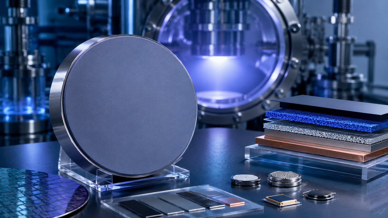
An ITO sputtering target is a solid, highly dense ceramic block or cylinder used as the source material in Physical Vapor Deposition (PVD) systems, specifically in magnetron sputtering. Inside a vacuum chamber, the target is bombarded by ionized gas (usually Argon), which ejects (sputters) ITO atoms into the vacuum to coat a substrate, forming a microscopic thin film.
Chemical Composition and Crystal Structure
ITO is a solid solution of Indium Oxide ($\text{In}_2\text{O}_3$) and Tin Oxide ($\text{SnO}_2$). The industry standard and most widely utilized composition is 90 wt% $\text{In}_2\text{O}_3$ and 10 wt% $\text{SnO}_2$.
In its crystalline form, ITO adopts a bixbyite structure. The addition of Tin ($\text{Sn}^{4+}$) substitutes Indium ($\text{In}^{3+}$) in the crystal lattice. Because Tin has a higher valency, it acts as an n-type electron donor. This doping mechanism, combined with naturally occurring oxygen vacancies ($\text{V}_\text{O}$), provides ITO with its free charge carriers.
Key Optoelectronic Properties
The unique value of ITO lies in its dual nature:
- Electrical Conductivity: High carrier concentration ($n > 10^{21}\text{ cm}^{-3}$) allows ITO to achieve ultra-low electrical resistivity, often dropping below $1.5 \times 10^{-4}\ \Omega\cdot\text{cm}$ in highly optimized thin films.
- Optical Transparency: ITO possesses a wide optical bandgap ($E_g \approx 3.75\text{ eV}$). Because visible light photons ($1.8\text{ eV}$ to $3.1\text{ eV}$) lack the energy to excite electrons across this bandgap, the material remains highly transparent ($>85\%$) in the visible spectrum.
(For deeper reading on the physics of Transparent Conductive Oxides, refer to fundamental research aggregates on platforms like ScienceDirect.)
2. How High-Purity ITO Sputtering Targets Are Manufactured
The performance of an ITO target is dictated by its purity, density, and microstructural uniformity. At Thin Film Materials (TFM), our state-of-the-art manufacturing process guarantees premium quality. The creation of a high-density ceramic target involves several rigorous metallurgical and ceramic processing steps:
Phase 1: Powder Mixing and Calcination
The process begins with ultra-high purity (>99.99%) $\text{In}_2\text{O}_3$ and $\text{SnO}_2$ powders. These powders are weighed to the exact 90:10 ratio and mixed using wet ball milling to ensure homogenous dispersion at the nanoscale. The slurry is then spray-dried and calcined. Calcination removes volatile impurities and initiates the solid-state reaction between the indium and tin oxides.
Phase 2: Consolidation and Sintering
Because ITO targets must withstand high-power bombardment without cracking or generating particles, achieving maximum theoretical density is critical. Two primary methods are used for consolidation:
- Cold Isostatic Pressing (CIP) followed by High-Temperature Sintering: The powder is shaped under uniform fluid pressure at room temperature, then sintered in oxygen-rich environments at temperatures exceeding $1500^\circ\text{C}$.
- Hot Isostatic Pressing (HIP): Pressure and heat are applied simultaneously, resulting in targets with densities exceeding 99.5%, virtually eliminating internal voids.
Phase 3: Machining and Backing Plate Bonding
Ceramic ITO is extremely brittle. To interface safely with a PVD machine’s water-cooled magnetron cathode, the target must be bonded to a backing plate (usually Oxygen-Free High Thermal Conductivity Copper, OFHC). At TFM, we utilize proprietary Indium bonding technology. Indium provides superior thermal and electrical conductivity between the target and the backing plate, dissipating the extreme heat generated during plasma bombardment.
3. PVD Deposition Techniques for ITO Thin Films
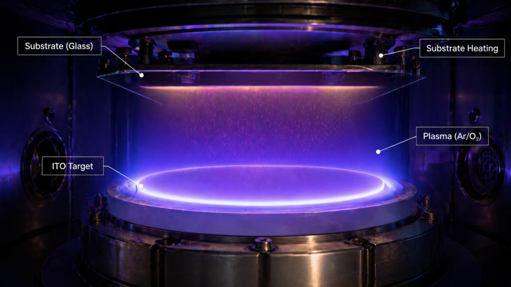
While thermal evaporation can be used, Magnetron Sputtering is the undisputed industry standard for depositing ITO thin films due to its excellent film adhesion, high density, and scalability.
DC Magnetron Sputtering
Because high-quality ITO ceramic targets are inherently conductive, Direct Current (DC) Magnetron Sputtering is the most common and economical method. DC sputtering allows for high deposition rates and is easily scalable for large-area coatings, such as Generation 10.5 LCD panel manufacturing.
RF Magnetron Sputtering
Radio Frequency (RF) Sputtering is occasionally utilized, particularly if the ITO target has lower conductivity or if the substrate is highly sensitive to charge buildup. However, RF deposition rates are generally lower than DC, making it more suited for specialized R&D rather than mass production.
The Role of Reactive Sputtering
During the sputtering process, some oxygen is lost to the vacuum pumps, leading to oxygen-deficient films that are highly conductive but optically dark (brownish or metallic). To counteract this, a precisely metered mixture of Argon ($\text{Ar}$) and Oxygen ($\text{O}_2$) gas is introduced into the chamber.
- Too little $\text{O}_2$: The film is conductive but opaque.
- Too much $\text{O}_2$: Oxygen vacancies are filled, making the film highly transparent but electrically resistive.
Process engineers must pinpoint the exact $\text{Ar}/\text{O}_2$ ratio to achieve the “sweet spot” of optimal conductivity and transmittance.
4. Key Applications of ITO Sputtering Targets
ITO thin films are the invisible backbone of modern electronics. If a device requires a surface to pass electricity while remaining entirely transparent, it likely utilizes ITO.
1. Flat Panel Displays (FPDs)
In Liquid Crystal Displays (LCDs) and Organic Light Emitting Diodes (OLEDs), ITO is deposited onto glass or flexible polymer substrates to act as the transparent electrode. It applies the necessary voltage to manipulate the liquid crystals or power the organic emission layers without obstructing the light generated by the display.
2. Photovoltaics and Solar Cells
In the renewable energy sector, ITO serves as a transparent front contact in various solar cell architectures, including Thin-Film, Heterojunction (HJT), and emerging Perovskite solar cells. High transmittance ensures maximum photon capture, while high conductivity minimizes series resistance, directly boosting the solar cell’s power conversion efficiency. For comprehensive data on solar cell efficiencies relying on TCOs, the National Renewable Energy Laboratory (NREL) is an excellent scientific resource.
3. Touch Panels (Capacitive and Resistive)
Your smartphone screen registers your touch thanks to a microscopic grid of ITO. When your conductive finger touches the screen, it disrupts the electrostatic field of the ITO grid, allowing the device’s processor to calculate the exact X-Y coordinates of your touch.
4. Smart Windows and Defogging Systems
In the automotive and aerospace industries, ITO films are applied to windshields and cockpit canopies. By passing an electrical current through the transparent ITO layer, the glass generates uniform Joule heating, efficiently clearing frost and fog without the need for visible heating wires.
5. Challenges in ITO Sputtering and Troubleshooting
Even with top-tier equipment, engineers frequently encounter process deviations. Understanding how the target behaves under plasma is essential.
Target Nodulation (Nodule Formation)
One of the most persistent issues in ITO sputtering is the formation of “nodules”—black, cone-shaped micro-protrusions on the target’s erosion track (the racetrack).
- Cause: Nodules form due to the re-deposition of back-sputtered material, sub-oxide formation, and localized thermal gradients.
- Impact: They disrupt the plasma, reduce the deposition rate, and can cause arcing. Micro-arcs can eject solid particles onto the substrate, resulting in fatal pinhole defects in displays.
- Solution: Nodulation can be significantly mitigated by using ultra-high-density (>99.5%) ITO targets manufactured by TFM. Higher density prevents localized overheating. Additionally, optimizing the magnetic field strength and using rotary (cylindrical) targets can drastically reduce nodule build-up.
Arcing and Target Cracking
- Arcing: Often a symptom of nodule buildup or target impurities. Arcs cause micro-explosions on the target surface.
- Cracking: Results from thermal shock. If the cooling water behind the backing plate is insufficient, or if the ramp-up power is applied too quickly, the brittle ceramic ITO will crack.
- Solution: Ensure flawless target-to-backing plate bonding (like TFM’s 100% ultrasonic-tested Indium bonds). Always adhere to a gradual power ramp-up schedule when igniting the plasma.
Sputtering Process Troubleshooting Matrix
| Problem | Potential Cause | TFM Recommended Solution |
| High Film Resistivity | Excess Oxygen in chamber; Substrate temp too low. | Reduce $\text{O}_2$ flow rate; Increase substrate heating to $250^\circ\text{C}-300^\circ\text{C}$ to improve crystallinity. |
| Poor Optical Transmittance | Oxygen deficiency; Metallic Indium precipitation. | Marginally increase $\text{O}_2$ partial pressure in the working gas. |
| Frequent Arcing | Nodule formation; Low target density; Impurities. | Switch to TFM >99.5% density targets; Clean chamber shields; Implement pulsed-DC power supply. |
| Target Cracking | Thermal shock; Poor backing plate bonding. | Follow slow power ramp-up ($<5\text{ W/cm}^2\text{ per min}$); Ensure water cooling is $>2\text{ GPM}$. |
6. Why Choose Thin Film Materials (TFM) for Your ITO Targets?
In the hyper-competitive B2B manufacturing landscape, your PVD process is only as reliable as your supply chain. Thin Film Materials (TFM) is not just a vendor; we are your strategic materials partner.
Here is why industry leaders in optoelectronics and photovoltaics choose TFM:
1. Uncompromising Purity and Density
Our ITO targets boast a purity of 99.99% (4N) to 99.995% (4N5), ensuring that your thin films are free from efficiency-killing contaminants. Through proprietary hot isostatic pressing (HIP), we consistently achieve densities exceeding 99.5%. This guarantees uniform erosion, eliminates micro-voids, and drastically reduces nodule formation and arcing.
2. Custom Fabrication: Planar and Rotary Targets
Whether your system uses a small R&D planar cathode or a 3-meter-long industrial rotary cathode, TFM can deliver.
- Planar Targets: Available in rectangular, circular, and custom geometries, seamlessly bonded to copper, molybdenum, or titanium backing plates.
- Rotary (Cylindrical) Targets: For large-scale manufacturing, our monolithic and segmented rotary ITO targets offer up to 80% material utilization, massively reducing your cost-of-ownership compared to planar alternatives.
3. Flawless Indium Bonding Technology
A cracked target halts production. TFM utilizes specialized, void-free Indium metallic bonding. Every target undergoes rigorous Ultrasonic Non-Destructive Testing (NDT) to guarantee 100% bond coverage, ensuring optimal thermal transfer and mechanical stability under high power densities.
4. End-to-End Engineering Support
From recommending the optimal target geometry for your specific OEM equipment (Applied Materials, Leybold, Ulvac) to assisting with parameter optimization for maximum film transmission, our materials scientists are available to ensure your success.
7. Conclusion: The Future of TCOs and TFM’s Commitment
While researchers continue to explore alternative Transparent Conductive Oxides like AZO (Aluminum Zinc Oxide) and FTO (Fluorine-doped Tin Oxide), Indium Tin Oxide remains the undisputed champion for high-performance applications. Its unmatched combination of low sheet resistance, high transmittance, and chemical stability secures its place in the future of flexible OLEDs, next-generation solar panels, and smart glass.
To maintain a competitive edge, manufacturers must eliminate process variables. By sourcing high-density, ultra-pure ITO sputtering targets from Thin Film Materials (TFM), you ensure stable plasma, higher deposition rates, and superior thin-film quality.
Ready to optimize your PVD process? Contact TFM today to Request a Quote or speak directly with our materials engineering team about your specific ITO requirements.
8. Top 10 Frequently Asked Questions (FAQs) About ITO Sputtering Targets
Q1: What is the standard composition of an ITO target?
A: The most common industry standard is 90 wt% Indium Oxide ($\text{In}_2\text{O}_3$) and 10 wt% Tin Oxide ($\text{SnO}_2$). However, custom ratios (e.g., 95:5 or 97:3) can be manufactured by TFM upon request for specific high-mobility applications.
Q2: Why is the density of an ITO target so important?
A: Higher density (e.g., >99.5%) means fewer internal voids and trapped gases. This results in uniform sputtering, significantly less nodule formation, fewer arcs, and a drastically reduced risk of the target cracking under thermal stress.
Q3: Can I use DC sputtering for ITO targets?
A: Yes, DC Magnetron Sputtering is highly recommended and widely used because the 90:10 ITO ceramic is adequately electrically conductive. It offers faster deposition rates compared to RF sputtering.
Q4: What causes ITO targets to turn black (form nodules) during sputtering?
A: Nodules are formed by the re-deposition of lower-energy sputtered particles back onto the target’s erosion groove, often reacting to form sub-oxides. Using high-density targets and optimizing magnetic field profiles helps mitigate this.
Q5: What is the role of Oxygen gas in ITO deposition?
A: Oxygen ($O_2$) is introduced alongside Argon to compensate for oxygen lost during sputtering. It fine-tunes the balance between optical transparency (requires more oxygen) and electrical conductivity (requires oxygen vacancies).
Q6: Are rotary (cylindrical) ITO targets better than planar targets?
A: For high-volume manufacturing, yes. Rotary targets rotate during deposition, resulting in uniform erosion across the entire surface. They offer up to 70-80% material utilization, whereas planar targets typically only yield 25-35% before needing replacement.
Q7: How do I prevent my ITO target from cracking?
A: Prevent thermal shock by ramping up the power slowly (e.g., 5-10 Watts per minute for smaller targets). Also, ensure that your cooling water flow meets the OEM’s specifications and that the target is properly bonded to its backing plate.
Q8: Can TFM bond ITO targets to my existing backing plates?
A: Yes. TFM provides full metallic bonding services using premium Indium. We can also reclaim and clean your used backing plates to bond new ITO materials, saving you money.
Q9: What is the typical purity of TFM’s ITO targets?
A: TFM supplies ITO targets with standard purities of 99.99% (4N). For advanced semiconductor or ultra-high-efficiency PV applications, we can provide 99.995% (4N5) purity levels.
Q10: Can ITO films be deposited onto flexible plastic substrates?
A: Yes. However, because plastic substrates (like PET) cannot be heated to the high temperatures ($>250^\circ\text{C}$) usually required for optimal ITO crystallization, low-temperature sputtering parameters must be used, often resulting in amorphous ITO films with slightly higher resistivity.