Introduction
In thin-film engineering, materials are no longer chosen simply for what they are, but for what they can become once deposited. Antimony Indium Tin (AIT) sputtering targets sit firmly in this modern materials philosophy. Rather than offering a single, fixed property set, they provide a design space—a way for researchers and engineers to fine-tune electrical, optical, and functional behavior directly at the materials level.
As device performance requirements continue to rise in semiconductors, displays, sensors, and energy systems, the ability to precisely control film composition has become essential. Antimony, indium, and tin—each already well established in thin-film technology—form a particularly adaptable system when combined into a single sputtering target. The result is a deposition material that supports experimentation, optimization, and scalable production without forcing compromise.
A Closer Look at the Material System
Why Antimony, Indium, and Tin Work So Well Together
Each element in an Antimony Indium Tin sputtering target brings a distinct contribution, and the real value lies in how these contributions interact during film growth.
- Indium provides the backbone of electrical performance. Its ability to support high carrier mobility makes it a familiar choice in conductive and semiconducting thin films.
- Tin adds stability and process reliability. It helps regulate resistivity and improves film robustness, especially under thermal or electrical stress.
- Antimony acts as a powerful tuning element. Even small amounts can noticeably influence carrier concentration, band structure, and overall film response.
Together, these elements allow deposited films to move smoothly along the spectrum from conductive to semiconducting behavior—without changing deposition equipment or introducing post-process complexity.
Target Fabrication with Deposition in Mind
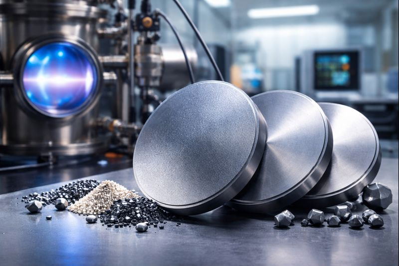
AIT sputtering targets are engineered not just for composition accuracy, but for predictable behavior in real sputtering systems. Depending on size and application, they may be produced using vacuum melting or powder-based consolidation techniques, followed by precision machining.
Key fabrication priorities include:
- Uniform elemental distribution across the entire target surface
- High density to ensure steady sputtering rates
- Controlled microstructure to minimize arcing and particle generation
For higher-power or long-duration runs, targets can be bonded to copper or titanium backing plates to improve thermal management and mechanical stability.
What Makes AIT Targets Stand Out in Practice
Composition as a Control Knob
One of the most appealing aspects of Antimony Indium Tin sputtering targets is that composition becomes a process variable, not a limitation. Adjusting Sb–In–Sn ratios allows users to directly influence:
- Electrical conductivity and resistivity
- Carrier concentration and mobility
- Film uniformity and reproducibility
This is particularly valuable in R&D environments, where rapid iteration and controlled comparisons are essential.
Stable Sputtering, Cleaner Films
Well-designed AIT targets offer stable plasma behavior across a wide range of sputtering conditions. This stability translates into:
- Consistent deposition rates
- Smooth film morphology
- Reduced defect density in deposited layers
For engineers scaling processes from lab to pilot production, this consistency helps eliminate surprises during transfer.
Flexibility Across Deposition Modes
AIT sputtering targets perform reliably in multiple PVD configurations, including DC and RF sputtering. They are also compatible with reactive sputtering environments, enabling controlled oxide or mixed-phase film formation without sacrificing target integrity.
Applications Across Technology Fields
Semiconductor and Microelectronic Structures
In semiconductor research and niche device fabrication, Antimony Indium Tin films are used as:
- Tunable conductive or semiconductive layers
- Interface films in multilayer stacks
- Functional electrodes where precise electrical behavior is required
Their adaptability makes them especially useful in exploratory device architectures.
Optical and Functional Coatings
Under controlled oxygen conditions, AIT-based films can form functional oxide layers that balance conductivity and optical performance. These coatings are relevant for displays, optoelectronic components, and smart surfaces where transparency and electrical response must coexist.
Energy and Emerging Devices
AIT thin films are increasingly explored in energy-related systems, including experimental photovoltaic structures and advanced sensor platforms. Their stability under operating stress supports long-term evaluation and device reliability studies.
Research-Driven Material Development
Universities and industrial R&D centers frequently select Antimony Indium Tin sputtering targets as platform materials—a starting point for systematic studies into composition-property relationships in thin films.
Technical Parameters (Typical)
| Parameter | Typical Value / Range | Why It Matters |
|---|---|---|
| Purity | 99.9% – 99.99% | Supports reproducible electrical and optical properties |
| Composition | Custom Sb–In–Sn ratios | Enables property tuning without hardware changes |
| Diameter | 25 – 300 mm (custom) | Fits both lab and production sputtering systems |
| Thickness | 3 – 10 mm | Affects sputter lifetime and process stability |
| Backing Plate | Optional Cu or Ti | Improves heat dissipation at higher power |
Comparison with Related Target Materials
| Material | Main Strength | Typical Use |
|---|---|---|
| Antimony Indium Tin | Highly tunable properties | Advanced semiconductor and functional films |
| Indium Tin | Established conductivity and transparency | Displays and optoelectronics |
| Tin Antimony | Mechanical and thermal stability | Functional and protective coatings |
| Pure Indium | Excellent low-temperature conductivity | Specialized electronic layers |
Frequently Asked Questions
| Question | Answer |
|---|---|
| Can I adjust the Sb–In–Sn ratio? | Yes, compositions can be tailored to specific electrical or optical targets. |
| Is this suitable for reactive sputtering? | Yes, it performs well in controlled oxygen atmospheres. |
| Are bonded targets available? | Copper or titanium backing plates can be supplied if required. |
| Is this more for research or production? | Both—commonly used in R&D and scalable pilot processes. |
| Can small quantities be ordered? | Yes, lab-scale targets and small batches are supported. |
Packaging
All Antimony Indium Tin Sputtering Targets are clearly labeled for traceability and quality control. Targets are vacuum-sealed and cushioned with protective materials to prevent contamination or damage during transport. Packaging options include reinforced cartons or export-grade wooden crates to ensure safe delivery worldwide.
Conclusion
Antimony Indium Tin sputtering targets are less about rigid specifications and more about possibility. By combining three complementary elements into a single, well-engineered target, they give thin-film researchers and engineers the freedom to explore, optimize, and scale advanced coatings with confidence.
For applications where flexibility, stability, and compositional control matter, AIT sputtering targets offer a practical and forward-looking solution.
For detailed specifications or a quotation, please contact sales@thinfilmmaterials.com.


