Introduction
Chromium Antimonide (CrSb) Sputtering Target is a specialized compound semiconductor and magnetic material used for advanced thin-film deposition research, particularly in spintronics, magnetic semiconductor studies, and functional electronic materials.
Unlike conventional metallic sputtering targets such as chromium or titanium, CrSb targets provide a combined system of transition-metal magnetism and semiconductor characteristics. This unique combination makes chromium antimonide an attractive material for studying spin-dependent transport, magnetic ordering, carrier behavior, and next-generation electronic devices.
For thin-film researchers, selecting a suitable CrSb sputtering target requires more than confirming the chemical formula. Target composition, purity, density, microstructure, bonding configuration, and deposition compatibility all influence the quality and reproducibility of deposited films.
A properly specified CrSb target can help researchers achieve more consistent thin films with controlled composition, improved interface quality, and reliable experimental results.
This guide explains the properties of chromium antimonide, its thin-film applications, key sputtering considerations, and how to select the right CrSb sputtering target for research and development.
What Is Chromium Antimonide (CrSb)?
Chromium antimonide (CrSb) is an intermetallic compound consisting of chromium and antimony. It belongs to the family of transition-metal pnictides, materials that combine magnetic properties from transition metals with semiconductor-like electronic structures.
CrSb has attracted interest because chromium contributes magnetic characteristics while antimony influences the electronic structure and bonding environment. This combination creates opportunities for studying magnetic semiconductor behavior and spin-related phenomena.
In bulk form, CrSb has been investigated as a magnetic material with applications in fundamental condensed matter research. When deposited as thin films, its properties can be influenced by:
- Crystal orientation
- Film thickness
- Substrate selection
- Deposition temperature
- Stoichiometric control
- Defect concentration
- Annealing conditions
Because many CrSb applications depend on precise control of magnetic and electronic properties, high-quality sputtering targets are essential.
A CrSb sputtering target provides a controlled source material for depositing chromium antimonide thin films using techniques such as:
- RF magnetron sputtering
- DC sputtering (where applicable)
- Co-sputtering processes
- Research-scale physical vapor deposition systems
Key Material Properties of Chromium Antimonide
CrSb is studied primarily because of its combination of magnetic, electronic, and structural characteristics.
1. Magnetic Properties
One of the most important research interests in CrSb is its magnetic behavior.
Transition metals such as chromium contribute magnetic moments through partially filled d-electron states. In CrSb, these magnetic interactions combine with the electronic structure of the antimonide framework.
This makes CrSb relevant for:
- Magnetic semiconductor research
- Spin-dependent transport studies
- Magnetic ordering investigations
- Spintronic device concepts
For magnetic thin films, even small variations in composition or defects can affect:
- Magnetic ordering temperature
- Magnetic anisotropy
- Carrier concentration
- Domain structure
- Transport behavior
Therefore, target composition control is particularly important.
2. Semiconductor and Electronic Characteristics
CrSb is often investigated as a functional electronic material because of its electronic band structure.
Thin films may be evaluated for:
- Electrical conductivity
- Carrier transport
- Band structure engineering
- Interface effects
- Semiconductor heterostructures
In research environments, CrSb films are commonly combined with other materials to study multilayer structures and interface-driven phenomena.
3. Structural Sensitivity
Like many compound semiconductor materials, CrSb properties depend strongly on crystal structure and deposition conditions.
Important factors include:
- Phase purity
- Grain size
- Film texture
- Defect density
- Substrate interaction
- Thermal treatment
A sputtering target with poor density or inconsistent composition may introduce additional variables that make thin-film analysis more difficult.
Why Use CrSb Sputtering Targets for Thin-Film Deposition?
A sputtering target is not simply a raw material source. It directly affects deposition stability, film composition, and process repeatability.
For CrSb thin films, target quality influences:
Composition Stability
Chromium and antimony have different physical properties during deposition. Maintaining the intended Cr:Sb ratio is critical because deviations may affect:
- Phase formation
- Electrical properties
- Magnetic behavior
- Film uniformity
A high-quality CrSb target helps reduce composition fluctuation during sputtering.
Film Repeatability
Research projects often require multiple deposition runs under similar conditions.
A consistent CrSb target helps improve:
- Film-to-film consistency
- Experimental comparison
- Process optimization
- Device testing reliability
This is especially important for spintronic and magnetic-material research where small variations can significantly influence results.
Reduced Contamination Risk
High-purity CrSb targets reduce unwanted impurities that may interfere with:
- Electrical measurements
- Magnetic characterization
- Interface analysis
- Device fabrication
Common impurity concerns include:
- Oxygen
- Carbon
- Iron
- Nickel
- Copper
- Other metallic contaminants
For advanced research, impurity limits may be more important than the nominal purity value alone.
Applications of Chromium Antimonide Thin Films
1. Spintronics and Magnetic Semiconductor Research
One of the most important research areas for CrSb is spintronics.
Spintronic devices use electron spin in addition to charge transport. Compared with traditional semiconductor electronics, spin-based technologies may offer advantages in:
- Data storage
- Magnetic memory
- Logic devices
- Low-power electronics
CrSb is studied as a candidate material for understanding magnetic semiconductor behavior and spin-dependent phenomena.
Potential research applications include:
- Spin transport experiments
- Magnetic heterostructures
- Spin injection studies
- Magnetic tunnel structures
- Spin-dependent electronic devices
For these applications, film quality and composition control are critical.
2. Magnetic Thin-Film Studies
CrSb thin films are also used in fundamental magnetic research.
Researchers may investigate:
- Magnetic ordering
- Magnetic phase transitions
- Domain behavior
- Exchange interactions
- Magnetic anisotropy
Thin-film deposition allows researchers to modify material behavior through:
- Strain engineering
- Layer thickness control
- Interface design
- Substrate selection
A reliable CrSb sputtering target supports these experimental studies by providing a stable material source.
3. Semiconductor Heterostructures
CrSb may be combined with other semiconductor or magnetic materials to create multilayer structures.
Examples include:
- CrSb/semiconductor interfaces
- Magnetic multilayers
- Spin-filter structures
- Functional electronic stacks
In these systems, interface cleanliness is extremely important.
Potential issues caused by poor target quality include:
- Unwanted secondary phases
- Interface contamination
- Composition variation
- Increased defect density
4. Advanced Functional Thin Films
Beyond spintronics, chromium antimonide may be studied in broader functional-material research.
Possible areas include:
- Magnetic sensors
- Electronic materials
- Quantum materials research
- Novel semiconductor systems
- Condensed matter physics studies
Many of these applications remain research-oriented, requiring customized deposition conditions and carefully controlled materials.
Deposition Considerations for CrSb Sputtering Targets
Composition Control
For compound sputtering targets, maintaining the correct elemental ratio is one of the most important requirements.
When specifying a CrSb target, customers should consider:
- Chromium-to-antimony ratio
- Allowable composition tolerance
- Phase requirements
- Intended film properties
- Deposition method
A target designed for exploratory research may have different requirements compared with a target intended for device fabrication.
Purity and Impurity Management
High-purity CrSb targets are typically preferred for advanced thin-film applications.
Important considerations include:
| Impurity | Potential Influence |
|---|---|
| Oxygen | Can affect bonding, defects, and film chemistry |
| Carbon | May influence electrical behavior |
| Metallic impurities | Can affect magnetic and transport measurements |
| Moisture / surface contamination | May influence vacuum deposition stability |
For sensitive projects, customers should specify:
- Required purity
- Critical impurity limits
- Required analysis method
- Documentation requirements
Target Density and Microstructure
Density is an important factor for sputtering performance.
A dense CrSb target can provide:
- More stable plasma operation
- Lower particle generation
- More uniform erosion
- Improved target lifetime
Porosity or internal defects may lead to:
- Particle formation
- Local heating
- Unstable deposition
- Reduced reproducibility
For compound semiconductor targets, density control is especially important because the target material may be more brittle than metallic targets.
Substrate and Thermal Conditions
CrSb film properties depend strongly on deposition parameters.
Important parameters include:
- Substrate temperature
- Working pressure
- Sputtering power
- Target-to-substrate distance
- Film thickness
- Annealing conditions
- Substrate material
The CrSb target provides the material source, but final film properties depend on the complete deposition process.
CrSb Sputtering Target vs Related Materials
| Material | Main Characteristics | Typical Research Applications |
|---|---|---|
| Chromium Antimonide (CrSb) | Magnetic semiconductor / transition-metal pnictide material | Spintronics, magnetic thin films, electronic materials |
| Chromium (Cr) | Conductive metallic material with strong adhesion properties | Adhesion layers, optical coatings, metal films |
| Antimony (Sb) | Semiconductor element and chalcogen-related material | Semiconductor alloys, thermoelectric materials |
| Manganese Antimonide (MnSb) | Magnetic semiconductor with strong magnetic behavior | Spintronic and magnetic research |
| Iron Antimonide (FeSb) | Iron-based pnictide compound | Electronic and magnetic studies |
| Bismuth Telluride (Bi₂Te₃) | Thermoelectric and topological material | Thermoelectric devices, quantum materials |
CrSb should be selected when the chromium-antimony compound itself is required. Chromium and antimony elemental targets may provide more flexibility for co-sputtering, but they do not directly provide the same compound composition.
How to Select a Chromium Antimonide Sputtering Target
Before purchasing a CrSb target, customers should confirm the following specifications.
Material Requirements
Confirm:
- Chromium antimonide composition
- Required purity
- Composition tolerance
- Phase requirements
- Impurity limits
Target Geometry
Provide:
- Diameter
- Thickness
- Rectangular dimensions
- Hole pattern
- Step design
- Cathode compatibility
Custom geometry is often required for research deposition systems.
Bonding Requirements
CrSb targets may be supplied as:
- Unbonded targets
- Bonded assemblies
For higher-power applications, bonded targets may provide:
- Improved heat transfer
- Better mechanical support
- Reduced thermal stress
Required information includes:
- Backing plate material
- Bonding method
- Total assembly thickness
- Cooling requirements
Documentation Requirements
Depending on application needs, documentation may include:
- Certificate of Analysis
- Composition data
- Impurity analysis
- Dimensional inspection report
- Bonding records
- Quality documentation
Typical Technical Parameters
| Parameter | Typical Value / Range | Importance |
|---|---|---|
| Material | Chromium Antimonide (CrSb) | Defines deposited compound film source |
| Purity | 99.9% – 99.99% | Higher purity reduces contamination risk |
| Composition | Cr:Sb controlled stoichiometric ratio | Influences phase and thin-film properties |
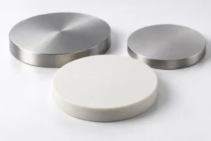
| Shape | Circular, rectangular, custom | Matches sputtering equipment |
| Diameter | 25 – 300 mm or custom | Ensures cathode compatibility |
| Thickness | 3 – 6 mm typical | Influences target lifetime |
| Density | High-density preferred | Improves sputtering stability |
| Bonding | Unbonded or copper-backed | Supports cooling and mechanical stability |
| Surface Finish | Machined / ground / cleaned | Supports consistent deposition |
| Documentation | CoA and inspection report | Provides traceability |
Manufacturing, Inspection & Documentation
CrSb sputtering targets require controlled manufacturing processes to maintain composition, density, and reliability.
Typical manufacturing steps include:
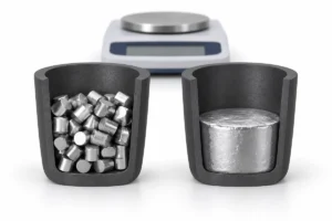
- Raw material preparation
- Compound synthesis
- Powder processing
- Forming
- Consolidation
- Machining
- Surface finishing
- Cleaning
- Inspection
- Packaging
Quality inspection may include:
- Composition verification
- Purity analysis
- Density evaluation
- Dimensional inspection
- Surface examination
- Visual inspection
For research applications, traceability and documentation help ensure reliable comparison between deposition experiments.
Packaging and Handling
Chromium Antimonide Sputtering Targets are carefully packaged to protect against:
- Surface contamination
- Mechanical damage
- Moisture exposure
- Edge chipping
Packaging may include:
- Clean protective bags
- Vacuum sealing where required
- Foam protection
- Export-safe cartons
- Wooden cases for larger assemblies
Each target is labeled for identification and quality control.
FAQ
| Question | Answer |
|---|---|
| What is a Chromium Antimonide sputtering target used for? | CrSb targets are mainly used for magnetic semiconductor, spintronic, and advanced thin-film research. |
| Can CrSb targets be customized? | Yes. Size, thickness, purity, bonding configuration, and packaging can be customized according to deposition requirements. |
| What sputtering methods can be used with CrSb targets? | RF magnetron sputtering and other PVD methods may be used depending on the equipment and film requirements. |
| Why is composition control important for CrSb? | The Cr:Sb ratio influences phase formation, electronic behavior, and magnetic properties of deposited films. |
| Are bonded CrSb targets available? | Bonded assemblies can be reviewed depending on target size, power requirements, and cooling conditions. |
| What documents are available? | CoA, composition data, impurity analysis, and dimensional inspection reports may be provided. |
Conclusion
Chromium Antimonide (CrSb) Sputtering Target is a specialized compound target designed for advanced thin-film research involving magnetic semiconductors, spintronics, and functional electronic materials.
Because CrSb film performance depends strongly on composition, purity, density, microstructure, and deposition conditions, target selection should consider more than material name alone.
A properly specified CrSb sputtering target helps researchers achieve improved deposition stability, better experimental repeatability, and more reliable thin-film characterization.
TFM supplies custom Chromium Antimonide Sputtering Targets with options for different purities, geometries, bonding configurations, inspection requirements, and research applications.
For detailed specifications and quotation, please contact: