Quick answer: A gallium nitride (GaN) sputtering target is a pre-compounded source used when a sputtering process is intended to deposit a Ga–N-containing film. It can simplify source-material handling compared with reactive sputtering from metallic gallium, but it does not guarantee film stoichiometry, phase, orientation, stress, electrical behavior, or optical quality. Target composition and form must be selected together with the power supply, cathode, backing and cooling arrangement, gas chemistry, substrate, thermal budget, film requirement, and validation plan.
What Is a GaN Sputtering Target?
A GaN sputtering target is a solid compound target that supplies gallium- and nitrogen-containing species to a physical vapor deposition process. Published experiments have used dense or pressed GaN targets, metallic gallium targets in reactive nitrogen-containing atmospheres, and other research-specific source configurations. Results from one route or chamber cannot be transferred to another without verification.
This article owns the engineering selection and validation intent. For current commercial forms and quotation options, use the Gallium Nitride Sputtering Target product page. For broader material navigation, use the Sputtering Targets catalog.
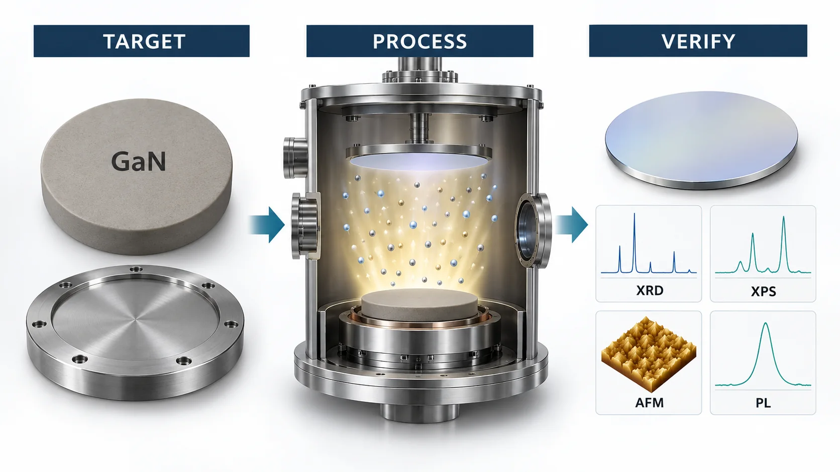
Choose the Deposition Route Before Specifying the Target
| Route | Why it may be evaluated | What must still be proven |
|---|---|---|
| Pre-compounded GaN target | A solid source with defined nominal chemistry; compatible with conventional target handling when cathode and power configuration are suitable | Electrical coupling, thermal behavior, erosion, particles, Ga:N transfer, phase, orientation, stress and functional properties |
| Metallic Ga or other reactive source route | Allows nitrogen incorporation to be controlled through a reactive process and is widely represented in research literature | Source handling, reactive-state stability, nitrogen activity, reproducibility, contamination and chamber-specific control |
| MOCVD, MBE, HVPE or another growth method | May be the established choice when epitaxy, heterostructures or device-grade crystal requirements dominate | Whether sputtering can meet the actual film and device acceptance criteria—not only cost, temperature or area objectives |
Published sputtering studies span polycrystalline films, oriented films and magnetron sputter epitaxy. “GaN film” is therefore not a single quality class. Define the required film outcome before treating any source route as equivalent.
Seven Inputs for GaN Target Selection
1. Film function and acceptance criteria
State whether the layer is exploratory, structural, optical, piezoelectric, electrically active, a buffer, or part of a device stack. Convert that function into measurable criteria such as phase, orientation, composition, thickness, stress, roughness, optical response, resistivity, carrier behavior, interface quality or defect limits. Do not use the target material name as a substitute for a film specification.
2. Target chemistry and documentation
Specify nominal GaN chemistry, intentional dopants if any, allowable impurities and the document required to support them. A catalog purity label alone does not define oxygen, carbon, metallic impurities, density, porosity, grain structure or lot-specific results. Ask which values are guaranteed, typical, measured per lot or available only by special inspection.
3. Geometry, cathode fit and erosion allowance
Provide diameter or rectangular dimensions, thickness, tolerances, edge treatment, cathode model, clamp or shield clearances, backing-plate interface and usable erosion requirement. Ceramic targets are sensitive to local mechanical constraint and uneven heat flow; nominal diameter alone is not enough to approve fit.
4. Electrical behavior and power delivery
The suitable power mode depends on the electrical response of the actual target, backing assembly, matching network and sputtering source. RF magnetron sputtering is frequently used for electrically resistive compound targets, but that observation is not a universal prescription. Confirm power-supply compatibility and qualify ramp, conditioning and steady operation on the actual tool.
5. Backing, bonding and cooling
Define whether a free-standing target or bonded assembly is required. For a bonded target, supply the backing material and drawing, bonding constraints, maximum permitted assembly thickness, cooling layout and acceptance method. Bond selection is an assembly decision; it must account for target brittleness, interface temperature, vacuum environment, thermal cycling and service procedure. See Target Bonding & Backing Plate Services.
6. Gas chemistry, substrate and thermal budget
Published GaN sputtering results change with nitrogen fraction, pressure, power, target-to-substrate geometry, substrate material, surface preparation, bias and temperature. These variables interact. A condition reported for glass, silicon or sapphire is evidence for that experiment—not a transferable recipe or a maximum/minimum for another chamber.
7. Inspection and traceability
Define the required target evidence before ordering: composition method, impurity list, density or porosity method, dimensions, flatness, visual criteria, bond inspection, backing identity, lot traceability, packaging and any witness documentation. If the project requires a batch certificate, say so explicitly; a typical specification sheet is not a batch certificate.
What Controls the Deposited Film?
Using a pre-compounded GaN target does not mean that the arriving flux or deposited film retains an ideal one-to-one composition. Preferential sputtering, gas-phase collisions, nitrogen activity, re-sputtering, substrate reactions and post-deposition exposure can change composition and bonding. Film structure also depends on surface mobility, bombardment, substrate orientation, buffer layers, thermal history and stress evolution.
| Observed issue | Possible contributors | Evidence to collect |
|---|---|---|
| Unstable plasma or arcing | Electrical coupling, conditioning, surface state, particles, pressure or matching | Forward/reflected power, arc log, pressure trace, target photographs and conditioning history |
| Target cracking or bond concern | Thermal gradient, cooling, local constraint, ramp, defect, bond void or shield contact | Crack map, erosion profile, cooling data, assembly drawing, bond inspection and power history |
| Nitrogen-deficient or oxygen-containing film | Gas chemistry, target surface, background species, leaks, chamber history, transfer or air exposure | XPS/RBS/ERDA or other composition data, gas record, residual-gas or leak information and handling history |
| Unexpected phase, orientation or stress | Substrate, buffer, temperature, energy flux, thickness, pressure, bias or thermal mismatch | XRD, Raman or curvature data, substrate/buffer record, thickness map and thermal history |
| Particles, roughness or nonuniformity | Target defects, redeposition, flaking, plasma instability, geometry, motion or shielding | Optical/SEM inspection, AFM or profilometry, particle map, erosion track and chamber photographs |
For a broader symptom-led workflow, use the Sputtering Target Troubleshooting Guide. If nitrogen is introduced reactively, also review Target Poisoning in Reactive Sputtering.
Build a Film Verification Plan
- XRD: identify phase and preferred orientation; use rocking curves or reciprocal-space methods only when the required structural question justifies them.
- XPS, RBS, ERDA or SIMS: evaluate composition, bonding or depth distribution with the method limitations and surface-preparation history recorded.
- SEM, AFM and profilometry: examine morphology, particles, roughness, thickness and uniformity at sampling locations defined before the run.
- Photoluminescence and optical spectroscopy: test optical response when it is relevant to the intended layer; a spectrum alone does not establish device suitability.
- Electrical testing: measure resistivity, carrier concentration and mobility only with an appropriate structure, contacts and method.
- Stress and adhesion: select measurements that fit the substrate and stack, and separate film stress from target/bond integrity.
Record chamber state, target history, substrate lot and preparation, run settings, thickness and sampling map with every result. Without that context, a “good” measurement cannot be reproduced or connected to the target specification.
GaN Sputtering Target RFQ Checklist
- Nominal GaN chemistry, intentional dopant and impurity limits
- Required purity evidence and lot-specific documentation
- Target shape, dimensions, tolerances, edge treatment and quantity
- Cathode model, clamp/shield clearances and drawing
- Free-standing or bonded configuration; backing material and geometry
- Bonding preference or operating constraints that must govern bond selection
- Power-supply type, matching network and known electrical limits
- Cooling arrangement, ramp constraints and intended duty profile
- Required density, porosity, microstructure or bond inspection method
- Film function, substrate/buffer, gas plan and key acceptance tests
- Packaging, cleaning, labeling and traceability requirements
Contact TFM with the drawing and the known process constraints. Unlisted purity, size, density, bonding, inspection or delivery requirements should be treated as review items rather than assumed capabilities.
Evidence Boundary
Evidence boundary: This guide does not specify a universal purity, density, grain size, target-manufacturing route, power mode, base pressure, working pressure, gas ratio, substrate temperature, target distance, deposition rate, film stoichiometry, crystal quality, device performance, target life or lead time. Published values cited below belong to the reported target, chamber, substrate and measurement conditions. Confirm the actual target record and qualify the film in the intended process.
Technical References
- Prabaswara et al., Review of GaN Thin Film and Nanorod Growth Using Magnetron Sputter Epitaxy, Applied Sciences (2020).
- Non-polar GaN thin films deposited on glass by conventional RF sputtering, Thin Solid Films (2019).
- GaN thin-film growth and characterization by magnetron sputtering, Surfaces and Interfaces (2021).
- High-quality GaN grown by reactive sputtering, Materials Letters (1991).
- Effect of growth conditions on GaN thin film by sputtering deposition, Journal of Crystal Growth (2007).