Introduction
Magnesium Oxide (MgO) wafers are a class of ceramic substrates renowned for their unique combination of high thermal stability, chemical inertness, and excellent dielectric properties. These qualities make MgO wafers indispensable in advanced electronics, thin film deposition, and optoelectronic applications. This article explores the fundamental characteristics, manufacturing methods, key applications, and market trends related to MgO wafers, aiming to provide a comprehensive reference for researchers, engineers, and procurement specialists.
1. Material Overview
1.1 What is Magnesium Oxide?
Magnesium Oxide (MgO) is an inorganic compound formed from the calcination of magnesium carbonate or magnesium hydroxide. In its single-crystal form, MgO exhibits a cubic crystal structure and is known for its high melting point, exceptional insulation properties, and chemical inertness.
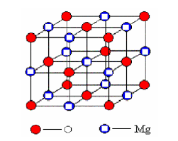
1.2 Crystal Structure
MgO crystallizes in the rock-salt structure (face-centered cubic), with a lattice constant of approximately 4.21 Å. This structure is highly stable and compatible with a variety of materials, making MgO a suitable substrate for heteroepitaxial growth.
1.3 Physical and Chemical Properties
- Melting Point: ~2852°C
- Thermal Conductivity: ~45 W/m·K at room temperature
- Dielectric Constant: ~9.8 (at 1 MHz)
- Band Gap: ~7.8 eV
- Hardness: ~5.5 Mohs
- Density: ~3.58 g/cm³
- Thermal Expansion Coefficient: ~13 × 10⁻⁶/K
- Optical Transparency: Transparent from UV to IR regions
These properties support high-temperature operations, excellent electrical insulation, chemical resistance, and compatibility with various deposition materials.
2. Manufacturing and Processing
2.1 Raw Material Selection
High-purity magnesium sources are essential for producing single-crystal MgO. Purity levels exceeding 99.95% are commonly required for electronics and photonics applications, particularly where defect-free films are critical.
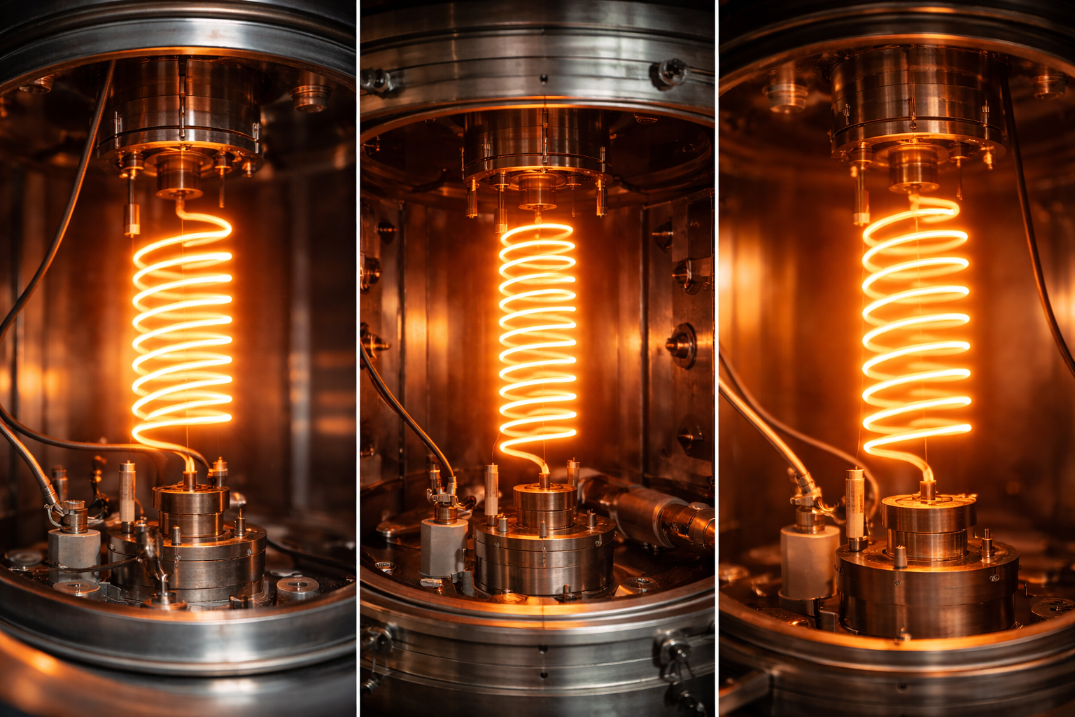
2.2 Crystal Growth Techniques
- Czochralski Method: A common method for growing large, high-quality single crystals. It involves dipping a seed crystal into molten MgO and slowly pulling it upwards while rotating.
- Bridgman Method: Employed for directional solidification of MgO crystals by gradually cooling the melt in a temperature gradient.
- Floating Zone Method: Offers ultra-high purity crystals by melting a small region with focused energy. It avoids contact with crucibles, reducing contamination.
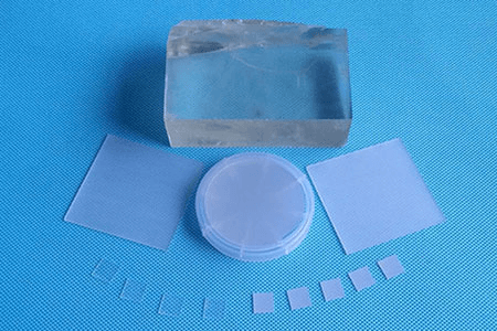
2.3 Wafering and Surface Preparation
After crystal growth, ingots are sliced into wafers of desired thickness (typically 0.3 to 1 mm) using diamond wire saws. The wafers are then lapped and polished to achieve mirror-like surfaces. Advanced chemical-mechanical polishing (CMP) processes can achieve surface roughness (Ra) < 5 Å for epitaxial use.
2.4 Crystallographic Orientations
Common wafer orientations include:
- (100): Standard for most deposition applications.
- (110): Used for specific anisotropic properties.
- (111): Preferred for certain epitaxial alignments, especially in perovskite oxide systems.
3. Applications of MgO Wafers
3.1 Thin Film Deposition Substrates
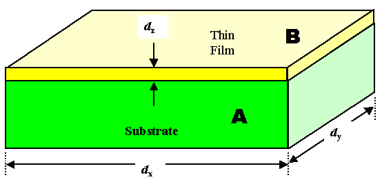
MgO wafers are widely used as substrates for physical vapor deposition (PVD), molecular beam epitaxy (MBE), and chemical vapor deposition (CVD). Their compatibility with various thin film materials enables their use in producing:
- High-temperature superconducting films (e.g., YBCO)
- Magnetic thin films (e.g., CoFe2O4, NiFe)
- Ferroelectric and piezoelectric films (e.g., BaTiO3, PbTiO3)
- Oxide semiconductors (e.g., ZnO, IGZO)
3.2 Spintronic Devices
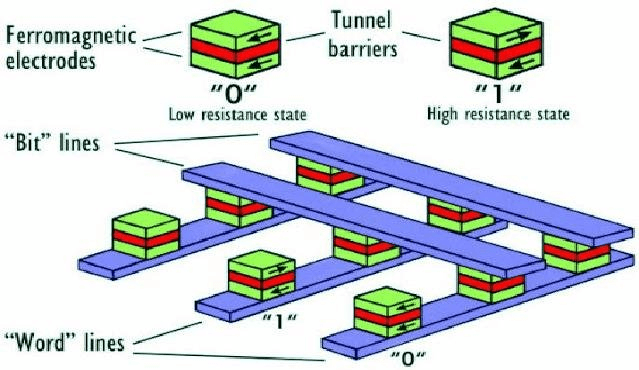
Due to their excellent tunnel barrier and magnetic isolation properties, MgO wafers serve as ideal substrates for magnetic tunnel junctions (MTJs) and spin valve structures. These are key components in MRAM (magnetoresistive random-access memory), magnetic sensors, and quantum spintronic systems.
3.3 Optical and Electro-Optical Applications
With high transparency in the visible to IR spectrum and low optical losses, MgO is utilized in:
- UV and IR detectors
- Solid-state laser host materials
- Electro-optic modulators
- Optical isolators
- Integrated photonic circuits
3.4 High-Temperature Electronics
The high thermal conductivity and dielectric strength of MgO wafers make them ideal for use with wide bandgap semiconductors like GaN, SiC, and AlN. These substrates are employed in:
- Power electronics
- High-frequency RF devices
- Harsh-environment sensors and ICs
3.5 Epitaxial Growth of Functional Oxides
MgO’s lattice constant and thermal stability enable it to serve as a template for the epitaxial growth of a wide range of functional oxide films, including:
- High-Tc superconductors
- Ferroelectric materials
- Multiferroics (e.g., BiFeO3)
- Transparent conducting oxides
4. Advantages Over Alternative Substrates
| Property | MgO | Sapphire (Al2O3) | SrTiO3 | Si |
|---|---|---|---|---|
| Lattice Constant (Å) | 4.21 | 4.76 | 3.905 | 5.43 |
| Melting Point (°C) | 2852 | 2050 | ~2000 | 1414 |
| Band Gap (eV) | 7.8 | 9.9 | 3.2 | 1.1 |
| Dielectric Strength | High | Moderate | Moderate | Low |
| Optical Transparency | Wide | Moderate | High | Poor |
| Chemical Inertness | Excellent | Good | Moderate | Low |
| Cost | Moderate | Low | High | Low |
| Thermal Stability | Excellent | Good | Fair | Poor |
MgO wafers offer an optimal balance of lattice compatibility, thermal endurance, chemical stability, and dielectric insulation—especially in oxide-based and high-frequency electronics. Compared to SrTiO3, MgO is chemically more stable and less hygroscopic, which contributes to easier storage and longer shelf life.
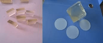
5. Common Specifications
- Diameter: 10 mm, 1 inch, 2 inches (custom sizes available)
- Thickness: 0.3 mm – 1 mm
- Orientation: <100>, <110>, <111>
- Surface Finish: Single-side or double-side polished (SSP/DSP)
- Purity: >99.95%
- Surface Roughness: <5 Å for high-end applications
- Packaging: Vacuum-sealed or nitrogen-purged boxes
- Edge Treatment: Beveled or rounded edges to reduce chipping risk
6. Storage, Handling, and Cleaning
MgO is hygroscopic and can absorb moisture from the air, leading to surface degradation or haze. Proper storage in a dry, inert atmosphere is essential to maintain surface quality.
Recommended Practices:
- Store in dry cabinets with nitrogen purge or desiccators
- Use clean-room gloves to prevent oil contamination
- Avoid rapid thermal changes to reduce cracking
Cleaning Procedures:
- Isopropyl alcohol (IPA) ultrasonic baths
- Dry nitrogen blow drying
- UV ozone cleaning for organic removal
- Avoid strong acids or bases to prevent surface etching
7. Market Trends and Outlook
7.1 Market Drivers
- Increasing demand for high-temperature semiconductors in EVs and aerospace
- Growth in oxide electronics, including smart sensors and IoT devices
- Expansion of MRAM and spintronics for AI hardware
- Rising interest in photonic integrated circuits and quantum optics
7.2 Regional Insights
- Asia-Pacific: Dominates in volume production and downstream device fabrication
- North America: Leads in R&D for emerging computing and energy systems
- Europe: Focused on photonic, biomedical, and clean energy devices
7.3 Competitive Landscape
The market is served by specialized manufacturers who offer MgO wafers with tight tolerances, advanced polishing, and customization options. Trends indicate growing demand for:
- Ultra-flat surfaces for epitaxy
- Wafer bonding for hybrid integration
- Low-defect densities for advanced device yields
8. Frequently Asked Questions (FAQs)
Q1: Can MgO wafers be used with GaN epitaxy?
Yes. MgO’s thermal and lattice properties support GaN deposition, although alternative substrates like sapphire and SiC are more commonly used for cost-performance balance.
Q2: Are MgO wafers safe to handle?
Yes, but precautions should be taken to avoid inhaling fine particles and to protect wafers from moisture, which can degrade the surface.
Q3: What is the main limitation of MgO wafers?
Hygroscopicity is the key limitation; improper storage can lead to surface clouding or degradation. Handling in controlled environments is recommended.
Q4: Is MgO biocompatible?
While MgO is generally considered bioinert and used in powder form in medical applications, the wafer form is not typically used in implants due to brittleness and lack of regulatory approvals.
Q5: Can MgO wafers be custom-manufactured?
Yes. Most suppliers offer customized diameters, orientations, thicknesses, and even pre-deposited buffer layers or coatings to meet specific application needs.
Q6: How does MgO compare with AlN as a substrate?
MgO is more cost-effective and easier to process, but AlN offers higher thermal conductivity. Selection depends on application-specific requirements.
Conclusion
Magnesium Oxide wafers are critical enablers in high-temperature electronics, advanced thin film deposition, and optoelectronics. Their distinctive combination of thermal, electrical, and chemical stability positions them as a versatile platform for emerging technologies, including quantum computing, spintronics, and oxide electronics.
As demand for high-performance materials continues to rise, MgO wafers are set to play an increasingly vital role in shaping the future of material science and device engineering. Their balance of cost, performance, and process compatibility makes them a smart choice for a variety of innovative applications.
Whether you’re a researcher developing next-gen devices or a buyer sourcing high-performance substrates, understanding the advantages and applications of MgO wafers can significantly improve your material selection and process outcomes.
Related Products
Magnesium Aluminate (Spinel) Substrate (MgAl2O4)