1. Introduction
In today’s ultra-advanced digital world, microelectronics is at the core of everything—from smartphones to satellites. The manufacture of microelectronic devices such as integrated circuits (ICs), thin-film transistors, LEDs, and solar cells requires highly controlled deposition and growth processes. Within this context, one unsung hero takes center stage: the microelectronics crucible.
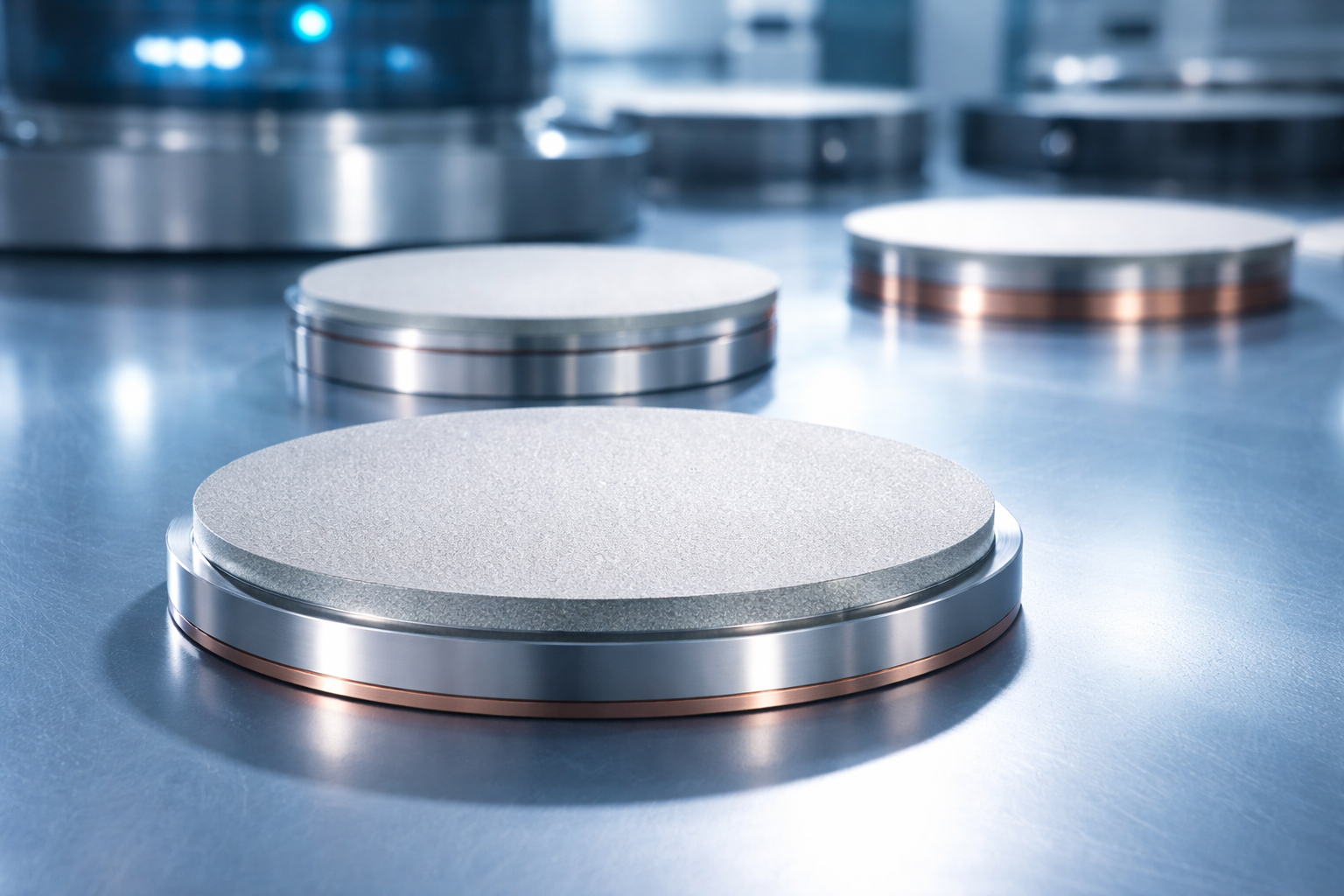
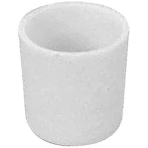
A microelectronics crucible is a specialized container used to hold, melt, or evaporate materials at high temperatures during semiconductor fabrication processes. Though often overlooked in favor of more glamorous technologies, the crucible is essential for enabling purity, uniformity, and stability in microfabrication. From thermal evaporation systems to crystal growth reactors, crucibles provide the physical environment where high-performance materials transition from solid to vapor or liquid states, ready to form the essential building blocks of modern electronics.
This article delves into the importance of microelectronics crucibles from a materials science and industrial perspective. It covers the selection of materials, process compatibility, emerging technologies, and the evolving role of crucibles in advanced electronics.
2. Material Selection for Microelectronics Crucibles
Crucible material selection is not a trivial decision. It directly affects the purity of the final product, the thermal efficiency of the process, and the compatibility with both the source material and the process atmosphere. Below are the most widely used materials in crucible manufacturing, each offering distinct advantages and challenges.
2.1 Quartz (Fused Silica)
Properties:
- Composition: SiO₂
- Melting Point: ~1,730°C
- Transparency to IR and UV radiation
- Very low thermal expansion
Applications:
Quartz crucibles are extensively used in the Czochralski method for silicon crystal growth, the dominant method for producing wafers for IC fabrication. They are also used in thermal evaporation systems for depositing metals like aluminum and titanium.
Advantages:
- Extremely high purity (up to 99.999%)
- Chemically inert in oxidizing environments
- Easy to fabricate into complex shapes
Limitations:
- Susceptible to devitrification at high temperatures
- Reacts with molten metals or certain dopants like phosphorus and boron
- Thermal shock sensitivity
2.2 Alumina (Al₂O₃)
Properties:
- High melting point: ~2,072°C
- High dielectric strength
- Excellent chemical resistance
Applications:
Alumina crucibles are ideal for oxide materials like ZnO, SnO₂, or In₂O₃. They are used in chemical vapor deposition (CVD) and resistive thermal evaporation systems. In laboratories, they are common for small-scale material testing and annealing.
Advantages:
- Withstands highly corrosive environments
- Maintains structural integrity under thermal stress
- Affordable and widely available
Limitations:
- Brittle, especially in thin-walled designs
- May react with highly reducing atmospheres
2.3 Boron Nitride (BN)
Properties:
- Sublimation point: ~2,973°C
- Very low thermal conductivity (unlike graphite)
- Lubricating properties
Applications:
BN crucibles are often used in metal-organic chemical vapor deposition (MOCVD), where reactive precursors require a chemically inert container. They’re also suitable for PVD of rare earths and chalcogenides like GeSbTe.
Advantages:
- Non-wetting and chemically inert
- Excellent thermal shock resistance
- Suitable for ultra-high-purity deposition
Limitations:
- Mechanically soft
- Not suitable for oxidizing atmospheres above 1,000°C
2.4 Graphite (with or without coatings)
Properties:
- High thermal conductivity
- Melting point above 3,000°C in inert atmosphere
- Can be coated with SiC, PyC, or BN for better stability
Applications:
Graphite crucibles are used in GaN and SiC growth, as well as in molten zone refining and vacuum smelting of high-purity metals.
Advantages:
- Excellent temperature tolerance
- High machinability for custom shapes
- Inexpensive for large-scale use
Limitations:
- Reactive in air at high temperatures
- Can release carbon contaminants if not coated
2.5 Refractory Metals (Tungsten, Tantalum, Molybdenum)
Properties:
- Exceptional melting points (up to 3,422°C for tungsten)
- High density and thermal stability
- Excellent resistance to thermal creep
Applications:
These crucibles are used in electron beam evaporation, MBE, and high-vacuum smelting of rare earth and transition metals. Tantalum is particularly popular for compound semiconductors such as GaAs and InP.
Advantages:
- Suitable for extreme vacuum and temperature environments
- High compatibility with high-purity processing
- Strong structural performance
Limitations:
- Oxidize easily above 400°C in air
- Require special handling and storage
- Costly compared to ceramics
2.6 Yttria-Stabilized Zirconia (YSZ) and Yttrium Oxide
Properties:
- Excellent resistance to plasma and ion bombardment
- High temperature capacity (>2,400°C)
- Electrical insulation under high temperature
Applications:
Used in MBE, PLD (Pulsed Laser Deposition), and advanced epitaxy processes. Yttria crucibles are ideal for oxide superconductors and ferroelectric materials.
Advantages:
- Chemically stable in both oxidizing and reducing environments
- Outstanding plasma resistance
- Minimal reaction with metal oxides and rare earths
Limitations:
- High cost
- Fragile in large sizes
3. Crucibles in Physical Vapor Deposition (PVD)
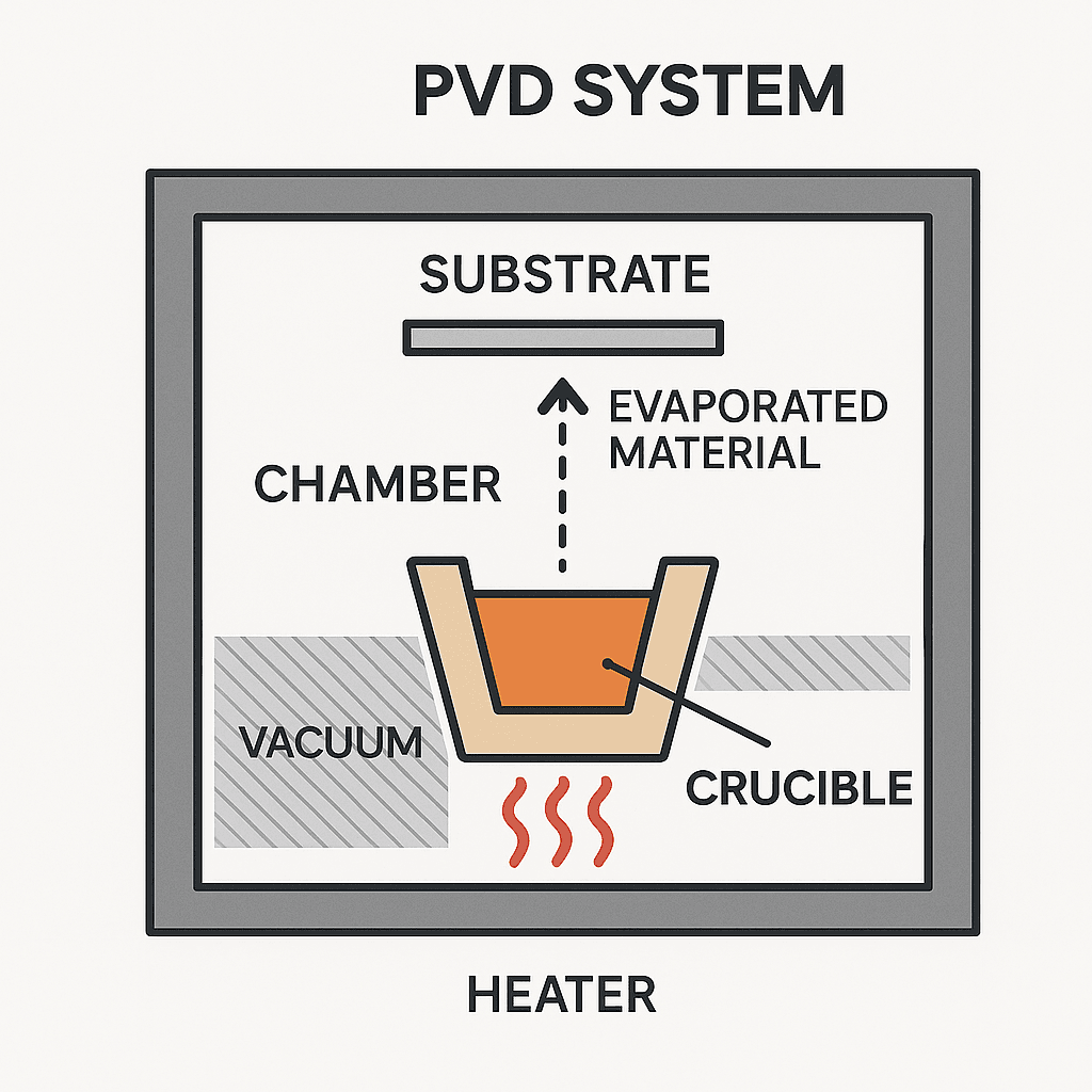
Physical Vapor Deposition (PVD) refers to a category of vacuum-based processes where a material is vaporized from a solid or liquid source and deposited as a thin film on a substrate. Crucibles are central to this operation, serving as the container for the source material.
3.1 Thermal Evaporation
In thermal evaporation, a resistive heater (often in the form of a tungsten basket or boat) heats a crucible containing metals such as aluminum, silver, gold, or titanium.
- Common Crucibles: Alumina, boron nitride, graphite, and refractory metal crucibles.
- Deposition Environment: High vacuum (~10⁻⁶ Torr).
- Key Considerations:
- Uniform heating to avoid spattering.
- Minimal interaction between crucible and metal (to avoid alloying or contamination).
- Non-wetting surfaces to retain melt shape.
Example: An alumina crucible used to evaporate gold in a precision optics coating process ensures that no crucible material dissolves into the molten gold, preserving optical clarity.
3.2 Electron Beam (E-Beam) Evaporation
In e-beam evaporation, a high-energy electron beam melts a target material in a water-cooled crucible (usually made of copper), but the molten material sits inside a liner crucible, also called a “crucible insert.”
- Common Liners: Yttria, tungsten, tantalum, graphite.
- Use Cases:
- High-melting-point materials (e.g., Ti, W, Mo, Si).
- Complex oxides or multilayers (e.g., ITO, ZnO:Al).
These liners must withstand focused heat, radiation, and cyclic heating while avoiding contamination of the vapor stream.
4. Crucibles in Chemical Vapor Deposition (CVD)
Chemical Vapor Deposition (CVD) processes involve the decomposition or reaction of gaseous precursors at elevated temperatures to form a solid film on the substrate. Though not all CVD processes require crucibles, in many low-pressure and atmospheric-pressure CVD systems, crucibles act as source containers for solid or liquid precursors.
4.1 Solid Precursor Delivery
In processes like ZnO deposition via CVD, solid zinc is often placed in a boron nitride or alumina crucible, heated to generate vapor that reacts downstream.
- Requirements:
- Precise temperature control to regulate vapor pressure.
- Low reactivity to prevent precursor degradation.
4.2 Metal-Organic CVD (MOCVD)
In MOCVD, often used to grow GaN and other III-V semiconductors, organometallic precursors like trimethylgallium (TMGa) are introduced. Though most precursors are gaseous or liquid, crucibles are still used for solid dopants or carrier evaporation.
- Specialty crucibles: BN and yttria-coated designs used for preventing contamination in group III-V systems.
5. Molecular Beam Epitaxy (MBE) Crucibles
MBE is a highly controlled deposition method where elemental beams are directed at a substrate under ultra-high vacuum (UHV) conditions.
Crucible Role in MBE:
- Contain ultrapure elemental sources (Ga, As, In, Sb, Bi, etc.)
- Enable controlled, shuttered fluxes of atomic/molecular species
- Operate at temperatures from 300°C to 1,500°C, depending on the material
Crucible Materials in MBE:
- Pyrolytic Boron Nitride (PBN): Preferred for its ultra-purity and non-reactivity.
- Graphite liners: Used in effusion cells.
- Yttria and Alumina: Used for oxide and rare earth deposition.
Key challenge: Prevent cross-contamination between source materials when growing complex heterostructures like quantum wells, superlattices, or high electron mobility transistors (HEMTs).
6. Crucibles in Crystal Growth Processes
Perhaps the most demanding application of crucibles is in single crystal growth, where the final wafer quality depends heavily on crucible stability and purity.
6.1 Czochralski Method for Silicon
This method dominates silicon wafer production. The process involves melting ultrapure silicon in a fused silica crucible, from which a seed crystal is slowly drawn.
- Operating Temp: ~1,420°C
- Challenges:
- Silica crucible slowly dissolves into molten silicon, requiring careful replacement.
- Any impurities introduced from the crucible affect wafer performance.
6.2 GaN and SiC Crystal Growth
In the case of wide bandgap semiconductors, crystal growth involves much higher temperatures and more reactive melts.
- Graphite crucibles coated with SiC or BN are used for sublimation or ammonothermal GaN growth.
- In Physical Vapor Transport (PVT) for SiC, crucibles must endure temperatures above 2,300°C.
Emerging Trend: Use of refractory metal crucibles (e.g., Ta, W) for bulk β-Ga₂O₃ growth, a promising material for high-power electronics.
7. Crucibles in OLED and Organic Semiconductor Fabrication
In OLED fabrication, crucibles are used for sublimating small-molecule organic compounds like Alq₃, rubrene, or dopants in vacuum thermal evaporation chambers.
Requirements:
- Extremely precise temperature ramping (±1°C)
- Uniform heating to prevent premature degradation
- Non-reactive to organic materials
Common Crucibles:
- Miniature molybdenum crucibles
- Alumina-coated metal boats
- Graphite-based crucibles for batch production
8. Crucibles in MEMS and Lab-on-Chip Systems
In microelectromechanical systems (MEMS) and lab-on-chip fabrication, crucibles are used at ultra-small scales for depositing thin film piezoelectrics, microheaters, and biosensors.
- Crucibles are miniaturized, often under 1 cm³ in volume.
- Used for materials like PZT (lead zirconate titanate) or ZnO.
- Heated with integrated microheaters or micro-coils.
As device footprints shrink, precision crucible engineering is becoming essential in pilot-scale and R&D environments.
9. Cross-Process Engineering Requirements
Regardless of the process, all crucibles used in microelectronics must meet strict criteria:
- Thermal Shock Resistance: Survive rapid heating and cooling cycles.
- Chemical Inertness: Avoid reacting with source or ambient gases.
- Mechanical Stability: Retain structural integrity under vacuum or gas pressure differentials.
- Dimensional Precision: For insertion into effusion cells, heaters, or source holders.
10. Cleanroom Protocols and Contamination Control
Microelectronics manufacturing requires ultra-clean environments, often ISO Class 5 or better, where the presence of even a single particle or contaminant atom can degrade device performance. Crucibles, as direct contact components in high-temperature material processing, must be designed, fabricated, packaged, and handled to meet strict cleanliness standards.
10.1 Sources of Contamination
- Particulate Shedding: Poorly sintered ceramic crucibles can flake or produce dust.
- Chemical Leaching: Some crucibles may leach dopants (e.g., Na, K) into high-purity melts.
- Surface Adsorption: Crucibles stored in ambient air can adsorb water or hydrocarbons.
10.2 Best Practices
- Cleanroom Packaging: Crucibles are double-bagged under nitrogen purge.
- Plasma Cleaning: Some users perform O₂ or Ar plasma surface treatments to eliminate adsorbed organics.
- Bake-out Protocols: Prior to use, crucibles are often baked at 400–800°C under vacuum to desorb volatiles.
Case Example: In high-volume OLED production, crucible liners are baked in Class 10 vacuum ovens and transferred via robotic arms to avoid particulate transfer.
11. Advanced Manufacturing of Crucibles
Producing crucibles for microelectronics is a high-precision, material-critical process. The fabrication techniques vary depending on material type but must achieve dimensional accuracy, structural homogeneity, and defect minimization.
11.1 Forming and Shaping Techniques
- Isostatic Pressing: Applied to ceramic powders (alumina, BN, YSZ) for uniform density.
- Slip Casting: For hollow, thin-walled shapes like quartz and alumina crucibles.
- CNC Machining: Especially for graphite, boron nitride, and refractory metals (W, Mo), often followed by polishing.
- Additive Manufacturing: In development for SiC, alumina, and complex liners (especially in custom R&D).
11.2 Sintering and Densification
- Sintering temperatures range from 1,600°C (alumina) to 2,200°C (BN, ZrO₂).
- Use of hot isostatic pressing (HIP) for void-free structures.
- Controlled atmosphere sintering (argon, hydrogen) to prevent oxidation or porosity.
11.3 Surface Treatments
- Chemical polishing for quartz crucibles to reduce nucleation sites.
- Pyrolytic Carbon (PyC) or SiC coatings on graphite for anti-contamination.
- Atomic Layer Deposition (ALD) coatings emerging for precision liner layers.
12. Industry Applications and Case Studies
12.1 Semiconductors
- Wafer Growth (CZ method): Fused silica crucibles are used in >95% of Si wafer production.
- E-beam and thermal evaporation: Crucibles hold source metals (Al, Ti, Cu) for metallization layers.
- MBE and CVD: Complex heterostructures (e.g., GaN/AlGaN for HEMTs) require crucibles for high-purity atomic sources.
Example: In a 300 mm fab, hundreds of crucibles are used weekly in deposition tools for barrier metals and dielectric layers.
12.2 Displays and OLEDs
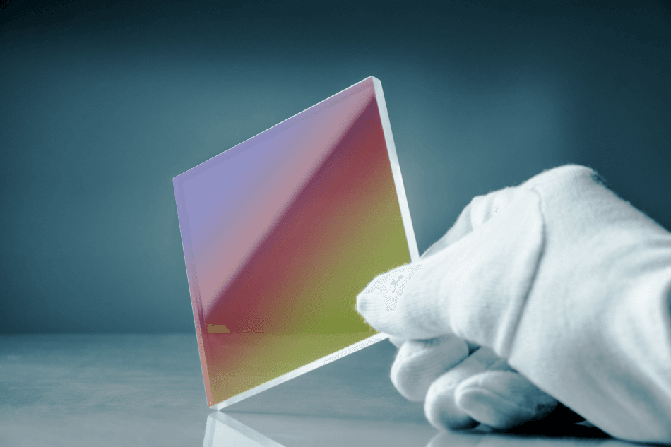
- OLED materials are highly sensitive to oxygen and metal impurities. Crucibles here must meet:
- <1 ppm metal contamination
- <10⁻⁶ g outgassing at 500°C
- Non-wetting surface finish to control evaporation rates
Brands like Samsung Display and BOE deploy crucibles made of BN or quartz composite in UHV OLED evaporation systems.
12.3 Photovoltaics (Solar Cells)
- Used for Si crystal growth, CdTe and CIGS absorber layer deposition.
- High-volume, cost-sensitive sector prefers crucibles that balance:
- Reusability
- High-temperature strength
- Low contamination
- Low cost per cycle
12.4 Quantum and Photonic Devices
- For quantum dots, superconductors, and topological insulators, ultra-pure materials are deposited from crucibles in MBE or PVD tools.
- BN, Ta, and PBN crucibles are used to prevent unintended doping or magnetic interference.
Example: In labs working on superconducting qubits, even sub-ppb magnetic contamination from crucibles must be avoided to preserve coherence time.
13. Future Trends and Emerging Technologies
13.1 Smart Crucibles
The next generation of crucibles may include embedded sensors and AI-driven monitoring:
- Thermocouples and IR sensors embedded into crucible walls
- Real-time measurement of melt composition
- Feedback to regulate source flux in closed-loop deposition systems
13.2 Green and Sustainable Manufacturing
As ESG (Environmental, Social, Governance) goals tighten:
- Recyclable crucibles are being explored (e.g., coated graphite).
- Waterless cleaning and dry plasma sterilization reduce chemical waste.
- Crucible leasing models (e.g., from OEMs like Plansee, POCO) help manage lifecycle impact.
13.3 High-Throughput R&D Crucibles
For materials discovery and prototyping:
- Miniaturized crucibles in combinatorial platforms allow screening of dozens of materials in parallel.
- Modular liner systems reduce downtime in university and fab labs.
13.4 Novel Materials for Crucibles
Research is ongoing into:
- Transparent ceramics (e.g., spinel, sapphire) for IR monitoring
- MAX phases and high-entropy ceramics for extreme environments
- Doped BN composites for improved thermal shock resistance
14. Conclusion
Microelectronics crucibles are critical infrastructure for modern materials processing. As electronics push toward:
- Smaller nodes
- Higher integration
- Broader material portfolios
- Tighter purity standards