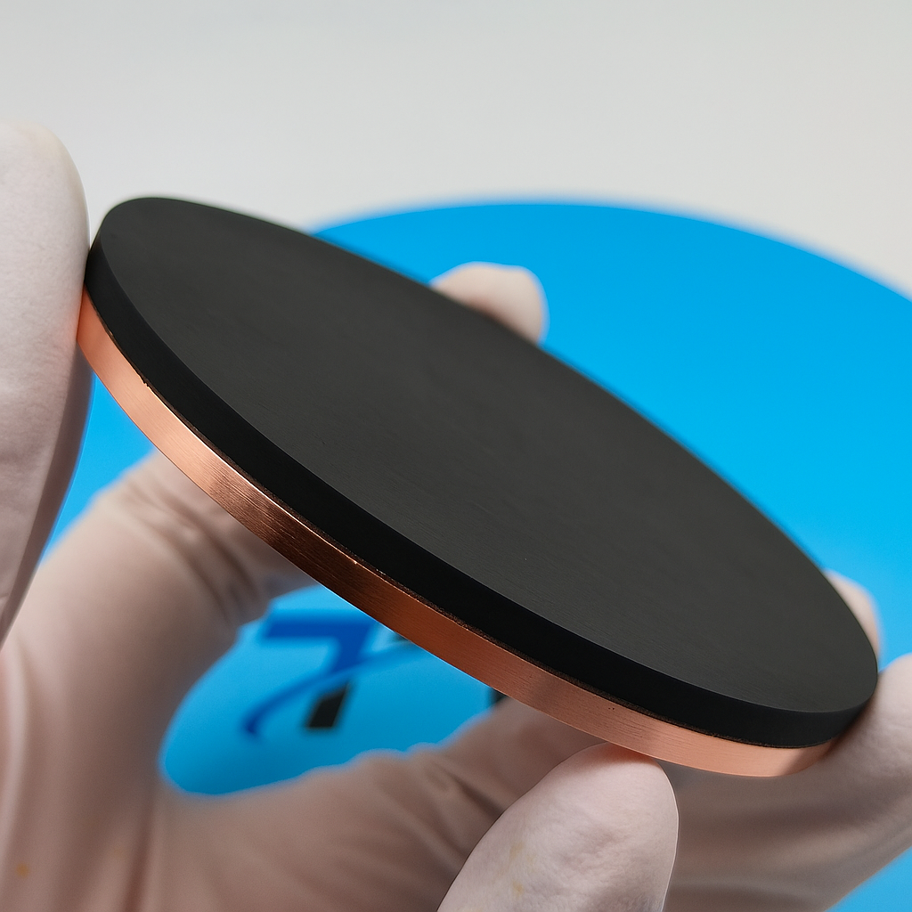

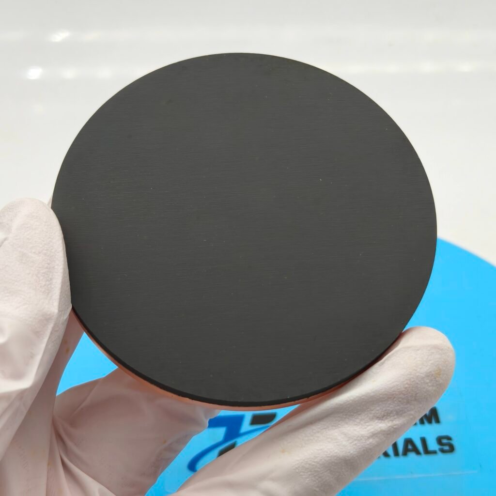


Nickel oxide (NiO) doped with lithium oxide (LiO₂) is becoming one of the most important functional oxide materials in modern thin-film engineering. When manufactured into a NiO–LiO₂ sputtering target, this material enables highly conductive, transparent, and stable p-type oxide films for a wide range of electronic and energy-related applications.
From transparent electronics and smart windows to gas sensors and thin-film batteries, Li-doped NiO sputtering targets offer exceptional performance advantages that pure NiO cannot achieve.
This article provides a comprehensive, keyword-rich overview covering composition, properties, deposition techniques, and real-world applications for NiO doped with LiO₂ sputtering targets.
What Is a NiO Doped with LiO₂ Sputtering Target?
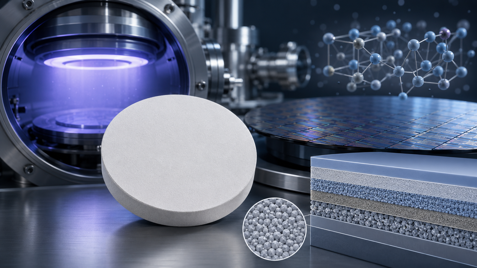
A NiO doped with LiO₂ sputtering target is a ceramic or composite sputter-deposition material made by adding lithium oxide to nickel oxide. Typical Li doping levels range from 1–10 mol%, depending on the electrical and optical performance required.
The target is used in:
- RF magnetron sputtering
- DC sputtering (with proper power control)
- Reactive sputtering systems
During deposition, lithium ions incorporate into the NiO lattice, improving carrier concentration and modifying film properties.
Why Use LiO₂-Doped NiO for Thin Films?
Pure NiO is a stable p-type oxide semiconductor but suffers from high resistivity and limited carrier mobility. Lithium doping solves these limitations.
Key Advantages of Li-Doped NiO Thin Films:
- Higher p-type conductivity
- Lower resistivity
- Improved transparency in the visible range
- Enhanced electrochromic performance
- Better catalytic activity
- Greater film uniformity and density
The combination makes Li-NiO an excellent material for electrochromic devices, TCO structures, sensors, and thin-film batteries.
Doping Mechanism of LiO₂ in NiO
Lithium ions (Li⁺) substitute for nickel in the NiO crystal lattice:
- Li⁺ replaces Ni²⁺
- Charge imbalance occurs
- Ni²⁺ becomes Ni³⁺ to compensate
This oxidation creates additional holes (positive carriers), dramatically improving conductivity.
Resulting material effects:
- Reduced bandgap (depending on doping level)
- Higher hole mobility
- Improved electrical performance
- Modified microstructure and grain size
This mechanism is why LiO₂-doped NiO sputtering targets are widely used for high-performance oxide electronics.
Manufacturing Process of NiO–LiO₂ Sputtering Targets
High-quality targets are crucial for stable sputter deposition. Manufacturers typically use:
1. Solid-State Sintering (Conventional Ceramic Processing)
- NiO and LiO₂ powders are weighed and mixed
- Ball milling ensures uniform dopant distribution
- Powders are pressed into molds and pre-sintered
- Final sintering occurs at 1200–1400°C
2. Hot Pressing or HIP (Hot Isostatic Pressing)
Improves density and eliminates microvoids, resulting in:
- Higher target density
- Better deposition uniformity
- Lower particle generation
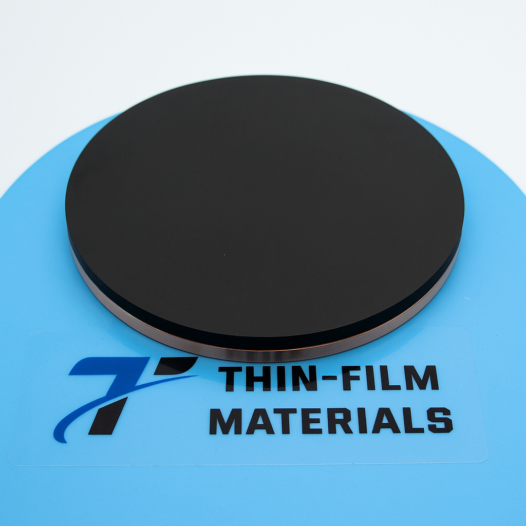
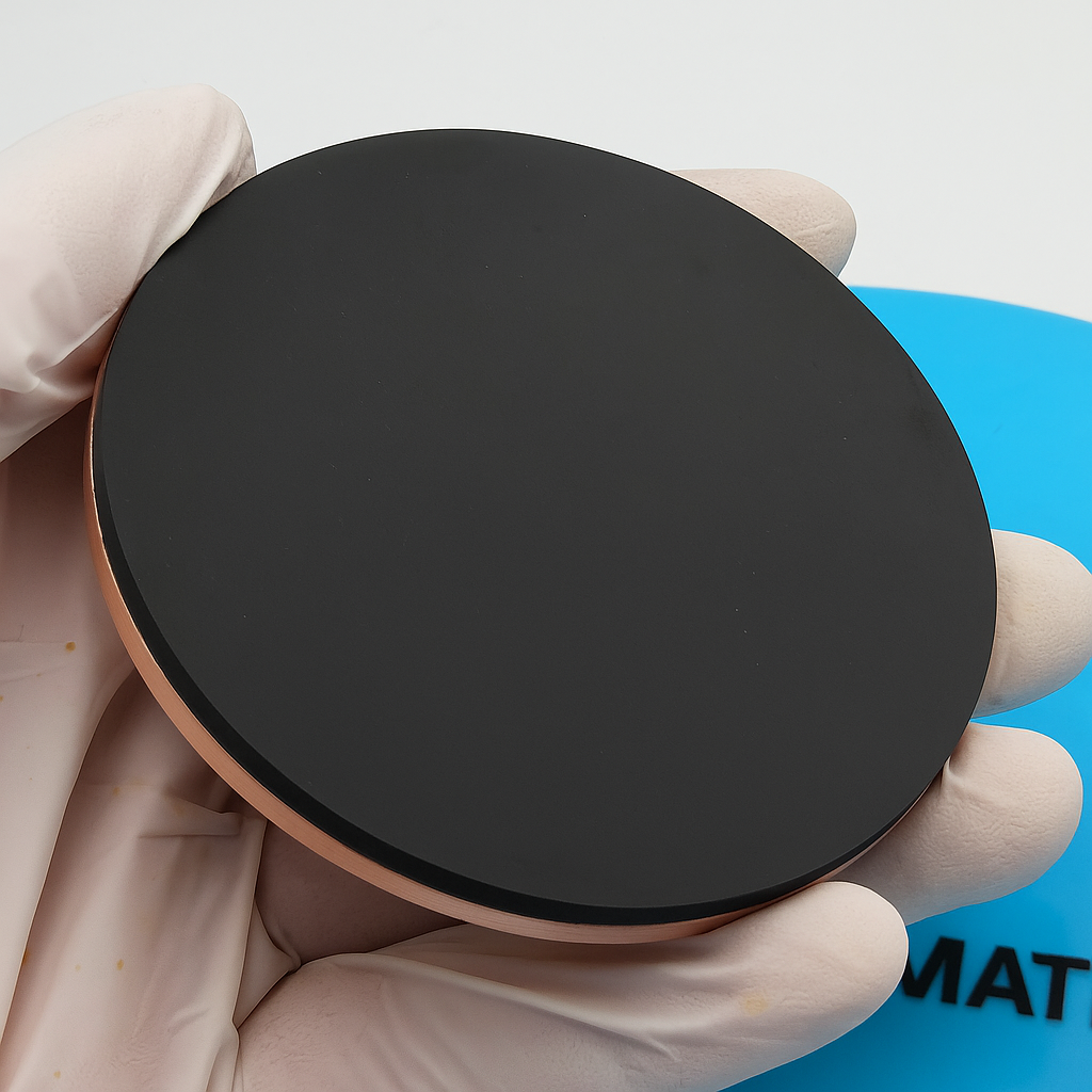
3. Bonding to Backing Plates
Large-area targets may be:
- Indium bonded
- Elastomer bonded
- Copper/Titanium backing plates
These improve heat transfer and prevent cracking during sputtering.
Sputtering Performance of Li-Doped NiO Targets
Lithium-doped NiO sputtering targets are compatible with:
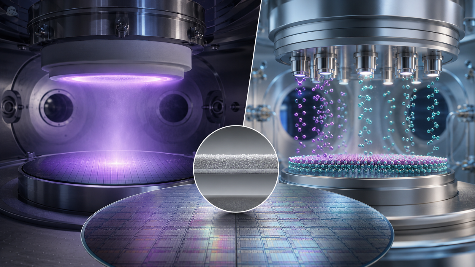
- RF magnetron sputtering (most common)
- Pulsed DC sputtering
- Reactive sputtering (in O₂/Ar mixes)
Typical Film Properties Achievable:
- Resistivity reduction by several orders of magnitude
- Optical transmittance >75% (depending on thickness)
- Smooth, compact microstructure
- Excellent adhesion on glass, ITO, Si, and sapphire
- High electrochemical stability
This makes Li-NiO films suitable for both research and industrial production.
Applications of NiO Doped with LiO₂ Sputtering Targets
1. Electrochromic Devices & Smart Windows
Li-doped NiO is one of the best p-type electrochromic materials, offering:
- High coloration efficiency
- Faster switching times
- Long cycling durability
Used in:
- Smart glass
- Architectural windows
- Automobiles and building energy systems
2. Transparent Electronics
Li-NiO is a promising p-type transparent conducting oxide (TCO) for:
- Transparent thin-film transistors (TFTs)
- Complementary oxide electronics (p-type NiO with n-type IGZO or ZnO)
3. Gas Sensors
Increased hole concentration improves detection of:
- Hydrogen
- Ethanol
- CO/NO₂
- VOCs
Li-doped NiO sensors show higher sensitivity and lower detection limits.
4. Lithium-Ion Batteries
Li-doped NiO thin films can be used as:
- Anode coatings
- Solid electrolyte interlayer films
- Protective layers for cathode materials
5. Photovoltaics & Photocatalysis
Li-NiO enhances:
- Hole transport in solar cells
- Photocatalytic degradation
- Water-splitting efficiency
6. Resistive Switching & Memristors
Li-NiO thin films exhibit stable:
- Switching voltages
- Filament formation
- Nonlinear conduction
Used in neuromorphic and memory-device research.
Choosing the Right NiO–LiO₂ Sputtering Target
When selecting a Li-doped NiO sputtering target, users should consider:
- Doping percentage (commonly 2%, 5%, 10%)
- Purity level (standard: 99.9% to 99.99%)
- Target density (higher density = better thin-film quality)
- Grain uniformity
- Single-piece or bonded construction
- Backing plate compatibility
High-density targets reduce arcing, increase deposition stability, and improve film uniformity.
Why NiO Doped with LiO₂ Is Becoming Essential
With the global demand for high-performance oxide thin films rising, Li-doped NiO sputtering targets offer a reliable route to:
- More efficient smart windows
- Faster electrochromic devices
- Better transparent p-type layers
- Next-generation sensors and batteries
- Emerging applications in IoT and flexible electronics
Its tunable conductivity, transparency, and chemical stability give it a competitive edge over many traditional p-type materials.