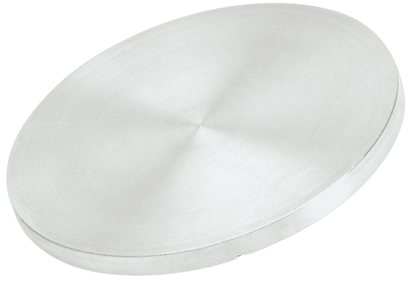
Aluminum Silicon Copper Sputtering Target Description
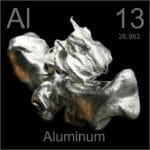 Aluminum, also known as aluminium, is a silvery-white, soft, non-magnetic, and ductile metal belonging to the boron group. Comprising about 8% of the Earth’s crust by mass, it is the third most abundant element after oxygen and silicon and the most prevalent metal in the crust. However, aluminum is less common in the Earth’s mantle. The primary ore of aluminum is bauxite. Due to its high reactivity, native aluminum is rare and typically found only in highly reducing environments; it is more commonly encountered in over 270 different mineral compounds.
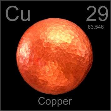 Copper is a chemical element whose name derives from the Old English word *coper*, which comes from the Latin *Cyprium aes*, meaning “metal from Cyprus.” First used around 9000 BC and discovered by people in the Middle East, copper has the chemical symbol “Cu” and is located in Period 4, Group 11 of the periodic table, within the d-block. Its atomic number is 29, and its relative atomic mass is 63.546, with the number in brackets indicating the uncertainty.
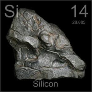 Silicon is a chemical element derived from the Latin *silex* or *silicis*, meaning flint. It was first mentioned in 1824 and observed by J. Berzelius, who also accomplished and announced its isolation. Silicon has the chemical symbol “Si” and is located in Period 3, Group 14 of the periodic table, within the p-block. Its atomic number is 14, and its relative atomic mass is 28.0855, with the number in brackets indicating the uncertainty.
Related Products: Aluminum sputtering target, Copper sputtering target.
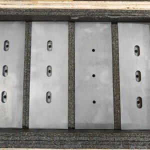
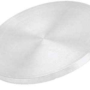
Aluminum Silicon Copper Sputtering Target Specifications
| Material Type | Aluminum Silicon Copper |
| Symbol | Al, Si, Cu |
| Available Sizes | Dia.: 2.0″, 3.0″, 4.0″, 5.0″, 6.0″ Thick: 0.125″, 0.250″ |
We also offer other customized shapes and sizes of the sputtering targets; please Contact Us for more information.
Aluminum Silicon Copper Sputtering Target Application
The Aluminum Silicon Copper Sputtering Target is used in thin film deposition, decoration, semiconductors, displays, LEDs, and photovoltaic devices. It also serves in functional coatings, optical information storage, glass coatings (including automotive and architectural glass), and optical communication technologies.
Aluminum Silicon Copper Sputtering Target Packing
Our Aluminum Silicon Copper Sputtering Targets are clearly tagged and labeled for efficient identification and quality control. We take great care to prevent any damage during storage and transportation, ensuring the targets remain in excellent condition.

Reviews
There are no reviews yet.