 MSDS File
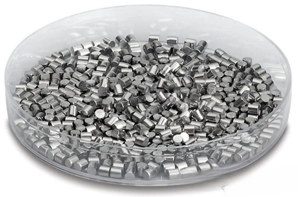
Aluminum Silicon Evaporation Materials
TFM offers high-quality aluminum silicon evaporation materials, which are alloys containing aluminum (Al) and silicon (Si). These materials are integral to various deposition processes, including semiconductor deposition, chemical vapor deposition (CVD), and physical vapor deposition (PVD). They are particularly useful in optical applications for wear protection, decorative coatings, and display technologies.
Applications
- Deposition Processes: Suitable for semiconductor deposition, CVD, and PVD.
- Optics: Ideal for wear protection, decorative coatings, and displays.
Packaging and Handling
We ensure that our aluminum silicon evaporation materials are carefully packaged to prevent any damage during storage and transportation. This meticulous handling helps preserve the products’ quality and integrity.
What We Supply
TFM provides a wide range of evaporation materials, including:
- Pure Metals and Alloys: Various compositions and forms.
- Ceramic Oxides: Including rare earth oxides such as Sc2O3, Y2O3, La2O3, and other ceramics like fluorides and nitrides.
- Forms: Available in tablets, granules, rods, and wires. Custom shapes and quantities can be provided upon request.
- Additional Components: We also supply evaporation sources, boats, filaments, crucibles, heaters, and e-beam crucible liners.
For current pricing and availability of evaporation pellets and other deposition materials not listed, please contact us with your inquiry.


Reviews
There are no reviews yet.