 MSDS File
Introduction
Antimony (Sb) Evaporation Materials are high-purity metallic sources widely used in thermal and electron-beam evaporation processes for semiconductor, optical, and functional thin film applications. As a group V element, antimony plays a critical role in compound semiconductors, phase-change materials, infrared devices, and alloy thin films. Controlled evaporation of Sb enables precise composition tuning in advanced deposition systems.
Detailed Description
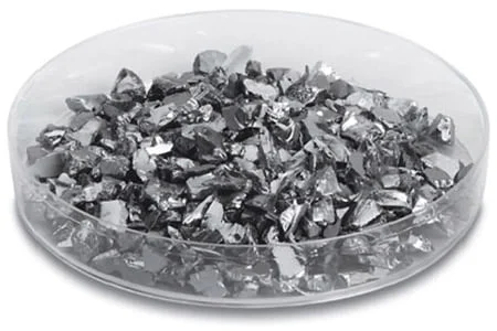
Our Antimony Evaporation Materials are refined from high-purity raw metal and processed into forms suitable for vacuum deposition systems. Due to antimony’s relatively low melting point and moderate vapor pressure characteristics, it is well suited for both thermal resistance heating and electron-beam evaporation under high vacuum conditions.
Careful control of metallic impurities and oxygen content is essential, as contaminants can significantly affect film conductivity, optical absorption, and compound semiconductor performance. Materials are available in shot, granule, pellet, and custom shapes to match different crucible types and evaporation sources. Particle size distribution can be tailored to ensure stable evaporation rates and minimize spitting during heating.
Applications
Antimony (Sb) Evaporation Materials are widely used in:
III–V compound semiconductor fabrication (e.g., InSb, GaSb)
Phase-change memory and chalcogenide materials
Infrared detector thin films
Alloying element in thin film deposition
Thermoelectric material research
Academic and industrial R&D in semiconductor physics
Technical Parameters
| Parameter | Typical Value / Range | Importance |
|---|---|---|
| Material | Antimony (Sb) | Group V semiconductor element |
| Purity | 99.9% – 99.999% | Reduces defect density in films |
| Form | Pellets / Granules / Shot / Custom | Compatible with evaporation sources |
| Particle Size | 1 – 6 mm (custom available) | Ensures stable evaporation |
| Melting Point | ~630 °C | Suitable for thermal evaporation |
| Evaporation Method | Thermal / E-beam | Matches PVD system requirements |
Comparison with Related Materials
| Material | Key Advantage | Typical Application |
|---|---|---|
| Antimony (Sb) | Essential Group V element | III–V semiconductors |
| Arsenic (As) | Narrow bandgap compounds | High-speed electronics |
| Bismuth (Bi) | Low melting point | Thermoelectrics |
| Selenium (Se) | Chalcogenide films | Phase-change materials |
FAQ
| Question | Answer |
|---|---|
| Can Sb purity be customized? | Yes, multiple purity grades up to 5N are available. |
| Is antimony suitable for thermal evaporation? | Yes, its melting point and vapor pressure make it compatible with thermal and e-beam methods. |
| How is evaporation stability ensured? | Controlled particle size and clean surface preparation reduce spitting and contamination. |
| How is the material packaged? | Vacuum-sealed or inert-gas packed in moisture-resistant containers. |
Packaging
Our Antimony (Sb) Evaporation Materials are meticulously tagged and labeled externally to ensure efficient identification and maintain high standards of quality control. We take great care to prevent any potential damage during storage and transportation, ensuring the materials arrive in optimal condition for immediate use.
Conclusion
Antimony (Sb) Evaporation Materials provide a dependable solution for high-purity thin film deposition in semiconductor and optoelectronic applications. With controlled purity, customizable forms, and stable evaporation characteristics, Sb is well suited for compound semiconductor growth, phase-change research, and advanced functional coatings.
For detailed specifications and a quotation, please contact us at sales@thinfilmmaterials.com.
| Material | Size | Quantity | Purity | Part Number |
| Antimony | 1mm - 3mm Pieces | 1 lb. | 99.999% | EVMSB501141 |
| Antimony | 1mm - 3mm Pieces | 25 g | 99.999% | EVMSB501141A |
| Antimony | 1mm - 3mm Pieces | 50 g | 99.999% | EVMSB501141B |
| Antimony | 1mm - 3mm Pieces | 100 g | 99.999% | EVMSB501141D |
| Antimony | 1mm - 3mm Pieces | 500 g | 99.999% | EVMSB501141T |
| Antimony | 3mm - 6mm Pieces | 25 g | 99.999% | EVMSB5036MMA |


Reviews
There are no reviews yet.