
 MSDS File
Arsenic Telluride Sputtering Target Description
Arsenic Telluride Sputtering Target is a specialized material used in sputtering, a technique for thin film deposition. In this process, Arsenic Telluride acts as the target material, which is bombarded with energetic particles, usually ions. This bombardment releases atoms from the target, which then deposit as a thin film onto a substrate, creating a coating with specific properties.
The Arsenic Telluride Sputtering Targets are distinguished by their excellent chemical stability, high electrical conductivity, thermal stability, and antioxidant properties. These attributes are enhanced by a precision design and a specialized manufacturing process. These characteristics make Arsenic Telluride Sputtering Targets highly valuable in the semiconductor industry and advanced electronic device manufacturing, where precise and reliable thin film deposition is essential for optimal device performance.
Related Product: Arsenic Triselenide Sputtering Target, Arsenic Trisulfide Sputtering Target
Arsenic Telluride Sputtering Target Specifications
| Compound Formula | As2Te3 |
| Molecular Weight | 532.64 |
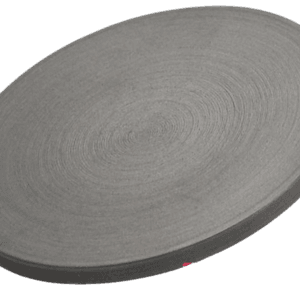
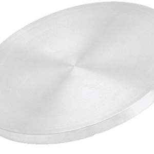
| Appearance | Black Target |
| Melting Point | 621 °C |
| Density | 6.5 g/cm3 |
| Available Sizes | Dia.: 1.0″, 2.0″, 3.0″, 4.0″, 5.0″, 6.0″ Thick: 0.125″, 0.250″ |
Arsenic Telluride Sputtering Target Handling Notes
Indium bonding is recommended for Arsenic Telluride Sputtering Targets due to its characteristics such as brittleness and low thermal conductivity. This material has low thermal conductivity and is susceptible to thermal shock, making indium bonding an effective choice to enhance its performance during sputtering processes.
Arsenic Telluride Sputtering Target Application
Arsenic Telluride Sputtering Targets find application in several fields:
- Semiconductor Industry: Used in thin film deposition to manufacture advanced electronic devices such as transistors and integrated circuits.
- Optoelectronics: Employed in the production of optoelectronic devices, including lasers and photodiodes.
- Optical Coatings: Applied in creating high-quality optical coatings for components like anti-reflective coatings and optical filters.
- Magnetic Storage: Utilized in the preparation of magnetic films to enhance the performance of magnetic storage devices.
- Nanotechnology Research: Used for creating nanoscale films and structures in nanotechnology research due to their precision and performance.
- Energy Storage: Applied in the development of high-performance electrode materials for new batteries and supercapacitors.
Arsenic Telluride Sputtering Target Packaging
Our Arsenic Telluride Sputtering Target is carefully handled during storage and transportation to maintain its quality and ensure it arrives in optimal condition.

Reviews
There are no reviews yet.