
Arsenic Triselenide Sputtering Target Description
The Arsenic Triselenide Sputtering Target, crafted from high-purity arsenic triselenide, is ideal for applications in semiconductors, optics, and photovoltaics. Utilizing sputtering technology, ultra-high purity metals or oxides are precisely deposited onto solid substrates, resulting in uniform, dense, and ultra-thin films.
Arsenic triselenide’s unique structure gives it remarkable optical properties, such as specific absorption and transmission characteristics in the infrared spectral range, along with non-linear optical properties. Additionally, it exhibits distinctive thermoelectric and electrical properties, making it a valuable material for advanced technological applications.
Related Product: Arsenic Trisulfide Sputtering Target
Arsenic Triselenide Sputtering Target Specifications
| Compound Formula | As2Se3 |
| Molecular Weight | 386.72 |
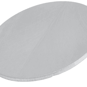
| Appearance | Black Target |
| Melting Point | 300℃ |
| Density | 4.75 g/cm3 |
| Available Sizes | Dia.: 1.0″, 2.0″, 3.0″, 4.0″, 5.0″, 6.0″ Thick: 0.125″, 0.250″ |
Arsenic Triselenide Sputtering Target Handling Notes
Indium bonding is recommended for the Arsenic Triselenide Sputtering Target because of the material’s brittleness and low thermal conductivity, which can present challenges during sputtering. These properties make the target susceptible to thermal shock. Indium bonding helps to mitigate these issues, enhancing the target’s stability and performance during the sputtering process.
Arsenic Triselenide Sputtering Target Application
Arsenic Triselenide Sputtering Targets offer unique properties that make them ideal for applications in optics and photovoltaics. Additionally, they are widely used in display technology through chemical vapor deposition (CVD) and physical vapor deposition (PVD) processes. For superior performance in your research and applications, select high-purity, high-quality Arsenic Triselenide Sputtering Targets from TFM.
Arsenic Triselenide Sputtering Target Packaging
Our Arsenic Triselenide Sputtering Target is meticulously handled throughout storage and transportation to ensure that it maintains its original quality and condition. We take every precaution to preserve the integrity of our products, so they arrive ready for optimal performance.
Get Contact
TFM offers Arsenic Triselenide Sputtering Targets in various forms, purities, sizes, and prices. We specialize in high-purity thin film deposition materials with optimal density and minimal grain sizes, which are ideal for semiconductor, CVD, and PVD applications in display and optics. Contact Us for current pricing on sputtering targets and other deposition materials that are not listed.


Reviews
There are no reviews yet.