
Introduction
Bismuth Antimony sputtering targets are alloy materials widely used in thin-film deposition for thermoelectric, electronic, and functional material research. By combining bismuth and antimony in controlled ratios, Bi–Sb alloy targets enable precise tuning of electrical conductivity, carrier concentration, and band structure. They are particularly important in low-temperature thermoelectric devices and advanced semiconductor research where material composition plays a decisive role in performance.
Detailed Description
Bismuth Antimony is a well-known solid-solution alloy system in which antimony is added to bismuth to modify electronic structure and transport behavior. Small changes in composition can significantly influence carrier mobility and thermoelectric efficiency, making compositional accuracy essential for thin-film applications.
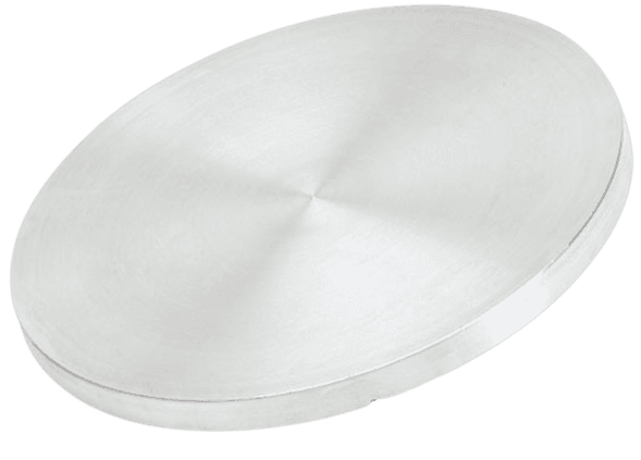
Our Bismuth Antimony sputtering targets are produced from high-purity bismuth and antimony using vacuum melting and alloy homogenization processes. The targets exhibit uniform composition, high density, and good mechanical integrity, ensuring stable sputtering rates and reproducible film properties. Careful control of microstructure helps reduce particle generation and compositional drift during deposition.
Bi–Sb targets are compatible with DC magnetron sputtering systems due to their metallic conductivity. Standard planar disc targets are available, with optional bonding to copper backing plates to improve thermal management and reduce stress during higher-power sputtering. Custom alloy ratios, dimensions, and bonding solutions can be provided to meet specific research or pilot-scale production needs.
Applications
Bismuth Antimony sputtering targets are commonly used in:
Thermoelectric thin films and devices
Topological insulator and quantum material research
Low-temperature electronic and sensing applications
Functional alloy thin films for semiconductor research
Academic and industrial R&D in advanced materials
Technical Parameters
| Parameter | Typical Value / Range | Importance |
|---|---|---|
| Material | Bismuth Antimony Alloy (Bi–Sb) | Defines electronic & thermoelectric behavior |
| Purity | 99.9% – 99.99% | Minimizes impurity-related defects |
| Composition | Custom Bi/Sb ratios | Tunes band structure & conductivity |
| Diameter | 1″ – 4″ (custom available) | Fits standard sputtering cathodes |
| Thickness | 3 – 6 mm | Affects sputtering lifetime |
| Density | High, alloy-controlled | Ensures stable sputtering rate |
| Backing Plate | Optional Cu | Improves heat dissipation |
Comparison with Related Materials
| Material | Key Advantage | Typical Application |
|---|---|---|
| Bismuth Antimony | Tunable electronic & thermoelectric properties | Thermoelectrics, quantum materials |
| Pure Bismuth | Low carrier density | Sensors, research films |
| Antimony | Semimetal behavior | Semiconductor applications |
| Bismuth Telluride | High thermoelectric efficiency | TE modules |
FAQ
| Question | Answer |
|---|---|
| Can the Bi/Sb ratio be customized? | Yes, alloy composition can be tailored to your specific requirements. |
| Is this target suitable for DC sputtering? | Yes, Bi–Sb targets are conductive and compatible with DC sputtering. |
| Are bonded targets available? | Yes, copper-bonded targets can be supplied upon request. |
| What applications most commonly use Bi–Sb films? | Thermoelectric devices and advanced electronic material research. |
Packaging
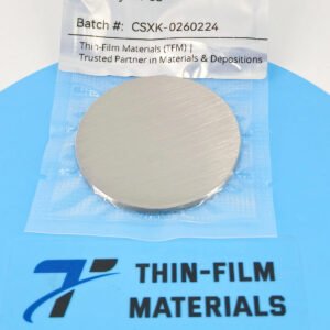
Our Bismuth Antimony Sputtering Targets are meticulously tagged and labeled externally to ensure efficient identification and strict quality control. Each target is vacuum-sealed and protected with shock-absorbing materials to prevent contamination or mechanical damage during storage and transportation.
Conclusion
Bismuth Antimony sputtering targets provide precise compositional control, stable sputtering performance, and reliable film quality for advanced thermoelectric and electronic thin-film applications. With flexible alloy customization and high manufacturing standards, Bi–Sb targets are an excellent choice for research-driven and specialized PVD processes.
For detailed specifications and a quotation, please contact us at sales@thinfilmmaterials.com.


Reviews
There are no reviews yet.