
 MSDS File
TFM provides high-purity bismuth(III) sulfide (Bi₂S₃) evaporation materials, a key component in producing high-quality films during various deposition processes. Our bismuth(III) sulfide materials are renowned for their purity, reaching up to 99.9995%, and are manufactured under strict quality control protocols to ensure exceptional reliability.
Related Products: Bismuth Evaporation Materials, Sulfide Ceramic Evaporation Materials
Bismuth(III) Sulfide Evaporation Materials Specification
| Material Type | Bismuth(III) sulfide |
| Symbol | Bi2S3 |
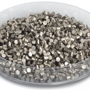
| Appearance/Color | Brown solid |
| Melting Point | 850 ˚C |
| Density | 6.78 g/cm3 |
| Purity | 99.9% ~ 99.99% |
| Shape | Powder/ Granule/ Custom-made |
Applications of Bismuth(III) Sulfide Evaporation Materials
Our bismuth(III) sulfide evaporation materials are employed in various deposition techniques, including semiconductor deposition, chemical vapor deposition (CVD), and physical vapor deposition (PVD). They are particularly useful in optical applications such as wear-resistant coatings, decorative finishes, and display technologies.
Packaging and Handling
We ensure that our bismuth(III) sulfide evaporation materials are thoroughly tagged and labeled for clear identification and quality control. Each package is carefully handled to prevent damage during storage and transportation.
Contact Us
TFM is a leading provider of high-purity bismuth(III) sulfide evaporation materials, offering them in various shapes such as tablets, granules, rods, and wires. Customized forms and quantities are available to meet specific needs. We also supply additional evaporation sources, boats, filaments, crucibles, heaters, and e-beam crucible liners. For pricing and further information on our products, please contact us.


Reviews
There are no reviews yet.