Generic selectors
Exact matches only
Search in title
Search in content
Post Type Selectors

VD0858 Bismuth Telluride Evaporation Materials, Bi2Te3

Catalog No.VD0858
MaterialBismuth Telluride (Bi2Te3)
Purity99.9% ~ 99.999%
ShapePowder/ Granule/ Custom-made

At TFM, we excel in producing and supplying top-quality high-purity bismuth telluride evaporation materials, along with a diverse range of other evaporation materials. Our offerings include both powder and granule forms, with customized options available to meet specific requirements.

Bismuth Telluride Evaporation Materials Overview

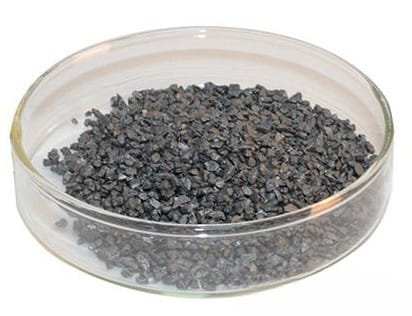
Bismuth telluride evaporation materials from TFM are high-purity ceramic materials with the chemical formula Bi2Te3. These materials are critical in various deposition processes to ensure the production of superior-quality films. TFM provides evaporation materials with purity levels up to 99.9995%, backed by rigorous quality control measures to guarantee reliability and performance.

Product Specifications

Material TypeBismuth Telluride
SymbolBi2Te3
Appearance/ColorGrey solid
Melting Point580 °C (1,076 °F; 853 K)
Density7.74 g cm−3
Purity99.9% ~ 99.999%
ShapePowder/ Granule/ Custom-made

Applications

Bismuth telluride evaporation materials are used in a variety of deposition techniques, including semiconductor deposition, chemical vapor deposition (CVD), and physical vapor deposition (PVD). They are particularly suited for optical applications such as wear protection, decorative coatings, and display technologies.

Packaging

Our bismuth telluride evaporation materials are carefully packaged in plastic vacuum bags to prevent damage during storage and transport, ensuring the materials retain their high quality. Each package includes a Certificate of Analysis (COA) to confirm the material’s specifications.

Contact Us

TFM specializes in producing high-purity bismuth telluride evaporation materials for use in semiconductors, CVD, PVD, and optical applications. Our expertise in engineering, manufacturing, and analysis allows us to deliver top-quality products. Contact us today for inquiries or further information.

Reviews

There are no reviews yet.

Be the first to review “VD0858 Bismuth Telluride Evaporation Materials, Bi2Te3”

Your email address will not be published. Required fields are marked *

FAQ

  • They are high‐purity substances (e.g. metals, alloys, or compounds) used in thermal or electron‐beam evaporation processes to form thin films on substrates.

  • Typically, they’re processed into a form (often ingots, pellets, or wires) that can be efficiently vaporized. Preparation emphasizes high purity and controlled composition to ensure film quality.

  • Thermal evaporation and electron-beam (e-beam) evaporation are the two main techniques, where material is heated (or bombarded with electrons) until it vaporizes and then condenses on the substrate.

  • Thermal evaporation heats the material directly (often using a resistive heater), while e-beam evaporation uses a focused electron beam to locally heat and vaporize the source material—each method offering different control and energy efficiency.

  • Key parameters include source temperature, vacuum level, deposition rate, substrate temperature, and the distance between the source and the substrate. These factors influence film uniformity, adhesion, and microstructure.

  • Evaporation generally produces high-purity films with excellent control over thickness, and it is especially suitable for materials with relatively low melting points or high vapor pressures.

  • Challenges include issues with step coverage (due to line-of-sight deposition), shadowing effects on complex topographies, and possible re-evaporation of material from the substrate if temperature isn’t properly controlled.

  • Common evaporation materials include noble metals (e.g., gold, silver), semiconductors (e.g., silicon, germanium), metal oxides, and organic compounds—each chosen for its specific optical, electrical, or mechanical properties.

  • Selection depends on desired film properties (conductivity, optical transparency, adhesion), compatibility with the evaporation process, and the final device application (semiconductor, optical coating, etc.).

  • Optimizing substrate temperature, deposition rate, and chamber vacuum are critical for ensuring that the film adheres well and forms the intended microstructure without defects.

  • Troubleshooting may involve checking the source material’s purity, ensuring stable source temperature, verifying the vacuum level, adjusting the substrate’s position or temperature, and monitoring deposition rate fluctuations.

While evaporation tends to yield very high purity films with excellent thickness control, it is limited by its line-of-sight nature. In contrast, sputtering can deposit films more uniformly on complex surfaces and is more versatile for a broader range of materials.


Shopping Cart
Scroll to Top