Introduction
Cadmium Sulfide Sputtering Target (CdS) is a critical II–VI compound semiconductor material widely used in thin-film deposition for optoelectronic and photovoltaic applications. With its direct wide bandgap and excellent optical response in the visible spectrum, CdS has long served as a benchmark buffer and window layer material in advanced semiconductor device structures. CdS sputtering targets enable precise, repeatable deposition of high-quality CdS thin films under controlled PVD conditions.
Detailed Description
CdS sputtering targets are manufactured from high-purity cadmium sulfide powders synthesized with strict stoichiometric control. The powders are consolidated through carefully optimized pressing and sintering processes to achieve high density, uniform microstructure, and stable sputtering performance. These characteristics are essential for minimizing arcing, particle generation, and compositional deviation during deposition.
Compared with reactive sputtering approaches, using a compound CdS target allows direct film formation without introducing additional sulfur-containing gases, significantly simplifying process control and improving film reproducibility. CdS targets are typically operated under RF sputtering due to their semiconducting nature, enabling smooth plasma stability and uniform erosion profiles.
CdS thin films deposited from sputtering targets exhibit strong optical absorption near the band edge, high transparency in the visible region (when properly controlled), and excellent interface compatibility with absorber materials such as CdTe and CIGS. These properties make CdS targets indispensable in both industrial-scale production and research-level device optimization.
Applications
Cadmium Sulfide sputtering targets are commonly used in:
Thin-film solar cells: Buffer and window layers in CdTe and CIGS photovoltaic devices
Optoelectronics: Photodetectors, photoconductors, and light-sensitive devices
Semiconductor research: Wide bandgap semiconductor and heterojunction studies
Optical coatings: Controlled absorption and transmission layers
Thin-film sensors: Gas, light, and radiation-sensitive coatings
Technical Parameters
| Parameter | Typical Value / Range | Importance |
|---|---|---|
| Chemical Composition | CdS (Cadmium Sulfide) | Defines bandgap and optical response |
| Purity | 99.99% – 99.999% | Ensures low defect density in films |
| Stoichiometry | Cd:S ≈ 1:1 | Maintains electrical and optical stability |
| Diameter | 25 – 300 mm (custom) | Compatible with standard sputtering cathodes |
| Thickness | 3 – 6 mm (typical) | Influences target lifetime |
| Density | ≥ 95% of theoretical | Supports stable sputtering behavior |
| Bonding | Indium / Elastomer / Direct | Improves heat dissipation and mechanical integrity |
Comparison with Related Materials
| Material | Key Advantage | Typical Application |
|---|---|---|
| CdS | Ideal bandgap for buffer layers | CdTe & CIGS solar cells |
| ZnS | Cadmium-free alternative | Optical and eco-sensitive devices |
| ZnO | High transparency, conductivity | TCO and window layers |
| CdSe | Narrower bandgap | Photodetectors and optoelectronics |
FAQ
| Question | Answer |
|---|---|
| Can CdS sputtering targets be customized? | Yes, size, purity, density, and bonding can be tailored. |
| Is RF sputtering required for CdS? | RF sputtering is typically recommended due to CdS’s semiconducting nature. |
| How is cadmium safety handled? | Targets are sealed and handled under strict safety and compliance procedures. |
| How are CdS targets packaged? | Vacuum-sealed with moisture- and contamination-resistant protection. |
Packaging
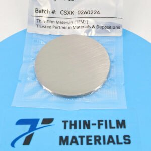
Our Cadmium Sulfide Sputtering Targets (CdS) are carefully labeled and vacuum-sealed to ensure traceability and consistent quality control. Protective cushioning and export-grade packaging are used to prevent mechanical damage and contamination during storage and international transportation.
Conclusion
Cadmium Sulfide Sputtering Target (CdS) remains a cornerstone material for high-performance thin-film photovoltaics and optoelectronic devices. With controlled stoichiometry, stable sputtering behavior, and customizable configurations, CdS targets provide a reliable solution for both production-scale manufacturing and advanced research applications.
For detailed specifications and a quotation, please contact us at sales@thinfilmmaterials.com.
Related Product: Cadmium Sputtering Target


Reviews
There are no reviews yet.