
Calcium Sulfide Sputtering Target Description
The calcium sulfide sputtering target is a ceramic sputtering material made up of calcium and sulfur. This material is commonly used in various industrial applications, particularly in thin film deposition processes. It is utilized in the production of coatings for semiconductor, display, LED, and photovoltaic devices, as well as for decorative and functional coatings in the optical information storage space industry, glass coating industry, including automotive and architectural glass, and optical communication systems.
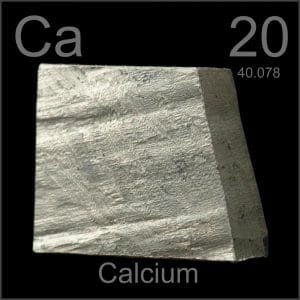 Calcium is a chemical element that derives its name from the Latin word ‘calx’, meaning lime. It was first mentioned in 1808 by Humphry Davy, who also achieved its isolation and announced it later that year. Represented by the symbol “Ca”, calcium has an atomic number of 20 and is situated in Period 4 and Group 2 of the periodic table, making it part of the s-block elements. The relative atomic mass of calcium is 40.078(4) Dalton, with the number in brackets indicating the measurement uncertainty.
Related Product: Calcium Sputtering Target
 Sulfur, also known as sulphur, is a chemical element with the symbol “S” and atomic number 16. It derives its name either from the Sanskrit word ‘sulvere’ or the Latin word ‘sulfurium’, both of which refer to sulfur. This element has been known and used since before 2000 BC, with early uses recorded by Chinese and Indian civilizations. Sulfur is located in Period 3 and Group 16 of the periodic table, making it part of the p-block. The relative atomic mass of sulfur is 32.065(5) Dalton, with the number in brackets indicating the uncertainty of this measurement.
Calcium Sulfide Sputtering Target Specification
| Compound Formula | CaS |
| Appearance | White to off-white target |
| Density | 4.82 g/cm3 |
| Melting Point | 2.5 g/cm3 |
| Molecular Weight | 72.14 |
| Available Sizes | Dia.: 1.0″, 2.0″, 3.0″, 4.0″, 5.0″, 6.0″ Thick: 0.125″, 0.250″ |
Calcium Sulfide Sputtering Target Application
The calcium sulfide sputtering target is utilized in a variety of applications, including thin film deposition for semiconductor, display, and LED technologies. It is also used in photovoltaic devices, functional coatings, and optical information storage industries. Additionally, calcium sulfide is applied in glass coating processes, particularly for automotive glass and architectural glass, as well as in optical communication systems. This material’s versatility makes it valuable in industries requiring durable and efficient coating solutions.
Calcium Sulfide Sputtering Target Packing
Our calcium sulfide sputter targets are meticulously tagged and labeled externally to facilitate efficient identification and maintain quality control. We take extensive precautions during handling and packaging to prevent any potential damage during storage or transportation, ensuring that the products arrive in optimal condition.
Get Contact
TFM offers Calcium Sulfide Sputtering Targets in various forms, purities, sizes, and prices. We specialize in high-purity thin film deposition materials with optimal density and minimal grain sizes, which are ideal for semiconductor, CVD, and PVD applications in display and optics. Contact Us for current pricing on sputtering targets and other deposition materials that are not listed.


Reviews
There are no reviews yet.