
 MSDS File
Introduction
CdInTe₄ pellet evaporation material is a specialized chalcogenide compound widely used in thin-film deposition for infrared, optoelectronic, and advanced semiconductor research. Thanks to its well-defined stoichiometry and favorable optical–electrical properties, CdInTe₄ is an important source material for fabricating compound semiconductor and functional thin films by thermal evaporation or electron-beam evaporation.
Detailed Description
Cadmium Indium Telluride (CdInTe₄) is a ternary telluride compound that combines the optoelectronic characteristics of cadmium telluride–based systems with indium-modified electronic behavior. When used as an evaporation material, precise compositional control is essential to ensure film uniformity and reproducibility.
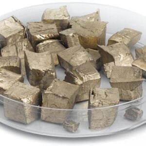
Our CdInTe₄ evaporation materials are manufactured from high-purity elemental cadmium, indium, and tellurium through carefully controlled synthesis and solidification processes. The material is processed into dense, uniform pellets to ensure stable evaporation rates and minimized spitting during deposition. Pellet geometry improves handling, loading efficiency, and material utilization compared with loose powders.
CdInTe₄ pellets are suitable for vacuum thermal evaporation and e-beam evaporation systems. The controlled microstructure and purity help maintain consistent vapor composition, which is critical for producing high-quality thin films with reliable optical absorption, electrical conductivity, and compositional uniformity. These materials are commonly used in research environments where precise film characteristics are required.
Applications
CdInTe₄ pellet evaporation materials are primarily used in:
Infrared and optoelectronic thin films
Compound semiconductor research and development
Photodetectors and sensor materials
Thin-film photovoltaic and photoactive layers
Chalcogenide semiconductor studies
Academic and industrial thin-film R&D
Technical Parameters
| Parameter | Typical Value / Range | Importance |
|---|---|---|
| Material | CdInTe₄ | Determines optical & electronic properties |
| Purity | 99.9% – 99.99% | Reduces contamination in deposited films |
| Form | Pellet | Ensures stable and clean evaporation |
| Pellet Size | 1–6 mm (custom available) | Compatible with various crucibles |
| Deposition Method | Thermal / E-beam evaporation | Matches standard vacuum systems |
| Moisture Sensitivity | Controlled handling required | Maintains material integrity |
Comparison with Related Materials
| Material | Key Advantage | Typical Application |
|---|---|---|
| CdInTe₄ | Tuned optoelectronic properties | IR & semiconductor thin films |
| CdTe | Mature material system | Photovoltaics, detectors |
| InTe | Narrow bandgap | Specialized electronic films |
| ZnTe | Wide bandgap | Optoelectronic coatings |
FAQ
| Question | Answer |
|---|---|
| Are CdInTe₄ pellets suitable for e-beam evaporation? | Yes, they are compatible with both thermal and e-beam evaporation systems. |
| Can pellet size be customized? | Yes, pellet dimensions can be tailored to your crucible or source design. |
| How is purity controlled? | High-purity raw materials and controlled synthesis are used. |
| What packaging is used? | Vacuum-sealed or inert-gas packaging to prevent oxidation and moisture uptake. |
| Is this material mainly for research use? | Yes, it is commonly used in R&D and pilot-scale thin-film development. |
Packaging
Our CdInTe₄ Pellet Evaporation Material is carefully labeled for full traceability and quality control. The pellets are vacuum-sealed or packed under inert atmosphere and protected with shock-absorbing materials to prevent contamination or damage during storage and transportation.
Conclusion
CdInTe₄ pellet evaporation material offers reliable composition, stable evaporation behavior, and high purity for advanced thin-film deposition. Its pellet form ensures ease of handling and consistent film quality, making it a dependable choice for optoelectronic and semiconductor research applications.
For detailed specifications and a quotation, please contact us at sales@thinfilmmaterials.com.

Reviews
There are no reviews yet.