 MSDS File
Introduction
Cerium Hexaboride (CeB₆) Evaporation Materials are high-performance compounds widely used in vacuum deposition processes and advanced electron emission technologies. Known for their exceptional thermionic emission properties, chemical stability, and high melting point, CeB₆ materials are essential in applications requiring stable electron sources and durable thin film coatings.
In Physical Vapor Deposition (PVD) systems, Cerium Hexaboride evaporation materials enable the formation of high-purity thin films with controlled composition and excellent stability. Due to their unique electronic and thermal properties, CeB₆ materials are frequently used in electron emission devices, vacuum electronics, and specialized coating applications.
Detailed Description
Cerium Hexaboride (CeB₆) is a refractory ceramic compound consisting of cerium and boron arranged in a stable cubic crystal structure. This material belongs to the family of rare-earth hexaborides, which are well known for their exceptional thermionic emission capabilities and high electrical conductivity compared with many other ceramic materials.
One of the defining characteristics of CeB₆ is its low work function, typically around 2.5 eV. This property allows electrons to be emitted efficiently at relatively lower temperatures compared with conventional tungsten emitters. As a result, CeB₆ is widely used as a cathode material in electron beam instruments and vacuum electronic devices.
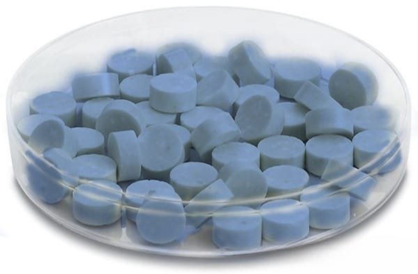
When supplied as evaporation materials, CeB₆ is typically available in the form of pellets, granules, or compact pieces suitable for electron beam evaporation or high-temperature thermal evaporation systems. The high melting point and thermal stability of CeB₆ allow it to maintain structural integrity during deposition processes.
CeB₆ also exhibits excellent chemical stability and resistance to contamination in vacuum environments. These characteristics help ensure consistent evaporation behavior and high purity in deposited films. Maintaining precise composition and high material purity is critical for applications where electronic properties must remain stable.
In addition to thin film deposition, CeB₆ materials are commonly used as electron sources in electron microscopes and ion sources due to their superior emission stability and long operational lifetimes.
Applications
Cerium Hexaboride evaporation materials are widely used in advanced vacuum and electronic technologies. Typical applications include:
Electron beam sources and thermionic cathodes
Thin film deposition using electron beam evaporation
Electron microscopy and analytical instruments
Vacuum electronic devices and ion sources
High-temperature conductive coatings
Advanced research in electronic and quantum materials
The combination of high electron emission efficiency and thermal stability makes CeB₆ particularly valuable in high-vacuum and high-temperature environments.
Technical Parameters
| Parameter | Typical Value / Range | Importance |
|---|---|---|
| Purity | 99.5% – 99.99% | Ensures stable evaporation and electronic properties |
| Chemical Formula | CeB₆ | Maintains correct compound stoichiometry |
| Density | ~4.7 g/cm³ | Influences evaporation behavior |
| Melting Point | ~2550 °C | Suitable for high-temperature evaporation |
| Work Function | ~2.5 eV | Enables efficient thermionic electron emission |
| Form | Pellets / Granules / Pieces | Compatible with evaporation sources |
Comparison with Related Materials
| Material | Key Advantage | Typical Application |
|---|---|---|
| Cerium Hexaboride (CeB₆) | Low work function and stable electron emission | Electron sources and vacuum electronics |
| Lanthanum Hexaboride (LaB₆) | Very strong thermionic emission | Electron microscopes |
| Tungsten (W) | High melting point and durability | Traditional electron emitters |
| Boron Carbide (B₄C) | High hardness and chemical stability | Protective coatings |
FAQ
| Question | Answer |
|---|---|
| What makes CeB₆ suitable for electron emission applications? | CeB₆ has a low work function and high electrical conductivity, allowing efficient electron emission at relatively low temperatures. |
| What deposition methods can use CeB₆ evaporation materials? | They are typically used in electron beam evaporation systems or high-temperature thermal evaporation processes. |
| What industries commonly use CeB₆ materials? | Electron microscopy, vacuum electronics, semiconductor research, and advanced materials science. |
| How should CeB₆ evaporation materials be stored? | They should be stored in clean, dry containers to prevent contamination and oxidation. |
| Are custom sizes or forms available? | Yes, CeB₆ evaporation materials can be supplied in various sizes and shapes depending on deposition system requirements. |
Packaging
Our Cerium Hexaboride Evaporation Materials are meticulously tagged and labeled externally to ensure efficient identification and maintain high standards of quality control. We take great care to prevent any potential damage during storage and transportation, ensuring the targets arrive in perfect condition.
Conclusion
Cerium Hexaboride (CeB₆) evaporation materials provide a reliable solution for thin film deposition and electron emission applications requiring high thermal stability and efficient electron generation. Their unique combination of low work function, high melting point, and chemical stability makes them essential for vacuum electronics, electron microscopy, and advanced research.
With customizable purity levels, material forms, and packaging options, CeB₆ evaporation materials support a wide range of high-performance vacuum deposition systems and electronic technologies.
For detailed specifications and a quotation, please contact us at sales@thinfilmmaterials.com.


Reviews
There are no reviews yet.