

Chromium Antimonide (CrSb) Sputtering Target Description
Chromium Antimonide (CrSb) Sputtering Targets are high-purity intermetallic materials engineered for precision thin film deposition in advanced magnetic, spintronic, and semiconductor applications. With a stoichiometric atomic ratio of 1:1 and purity up to 99.99%, CrSb targets deliver reliable performance in research and industry environments requiring stable magnetic and electronic properties.
Material Overview: What is CrSb?
CrSb is a binary compound composed of chromium (Cr) and antimony (Sb) in a 1:1 atomic ratio. It crystallizes in a NiAs-type hexagonal structure, exhibiting robust antiferromagnetic or ferromagnetic behavior depending on the growth conditions and temperature. Its unique combination of electronic and magnetic properties makes it a promising material for next-generation devices.
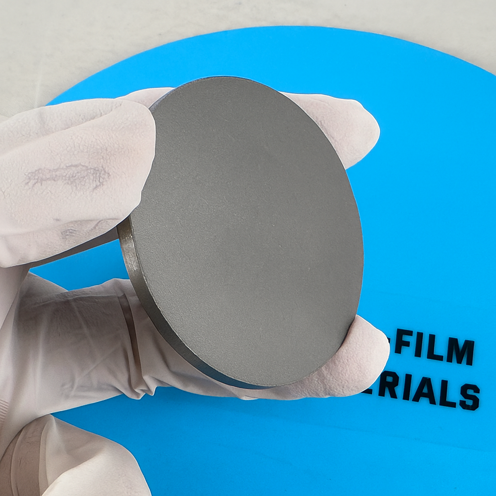
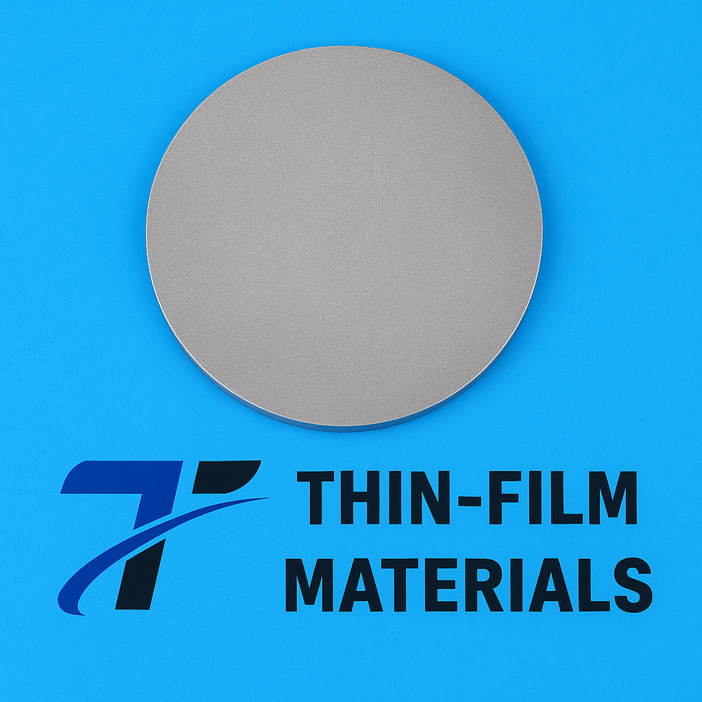
Chromium Antimonide Sputtering Target Specifications
| Property | Value |
|---|---|
| Chemical Formula | CrSb |
| Composition | 1:1 atomic ratio (Cr:Sb) |
| Purity | 99.99% (4N) |
| Appearance | Metallic gray to black, solid |
| Target Diameter | Ø50.8 mm (2 inches) |
| Target Thickness | 3 mm |
| Backing Plate | Copper (Cu), 2 mm thickness |
| Bonding Method | Indium bonding (standard) or custom on request |
| Packaging | Cleanroom-sealed under inert atmosphere |
CrSb Sputtering Target Applications
1. Spintronics and Magnetic Thin Films
CrSb is considered a half-metallic ferromagnet, meaning it can conduct electrons of one spin orientation while acting as an insulator for the opposite spin. This property is highly valuable in spintronic devices such as magnetic tunnel junctions (MTJs), GMR sensors, and spin transistors.
2. Semiconductor Research
Due to its narrow band gap and tunable carrier density, CrSb is of interest in developing magnetic semiconductors, topological materials, and quantum computing devices.
3. Magnetic Data Storage
CrSb films are being explored for high-density storage media, where spin-aligned materials enable faster and more stable data processing and retention.
4. Fundamental Material Science
CrSb sputtering targets are widely used in laboratories to study magnetotransport, crystal growth, and phase transition behaviors of intermetallic magnetic compounds.
Key Advantages of CrSb Sputtering Targets
High Purity (99.99%) ensures contamination-free deposition for research-grade films.
Excellent Magnetic Properties, suitable for spintronic and magnetic device fabrication.
Stable Thin Film Formation under various deposition techniques such as RF/DC magnetron sputtering and pulsed laser deposition.
Custom Sizes and Bonding Options available to meet specific system requirements.
Customization and Support
TFM offers Chromium Antimonide Sputtering Targets in a variety of sizes, thicknesses, and bonding configurations. Whether you’re exploring spintronic mechanisms or manufacturing prototype devices, our team can provide tailored CrSb solutions to match your equipment and project goals.


Reviews
There are no reviews yet.