
 MSDS File
Chromium(II) Silicide Evaporation Materials Description
Chromium(II) silicide (CrSi2) evaporation material from TFM is a high-purity silicide ceramic used in advanced deposition processes. Known for its chemical stability and performance, CrSi2 plays a crucial role in producing high-quality deposited films. TFM excels in delivering chromium(II) silicide with purity levels up to 99.9995%, ensuring reliability and superior quality through stringent quality assurance practices.
Specifications
| Material Type | Chromium disilicide |
| Symbol | CrSi2 |
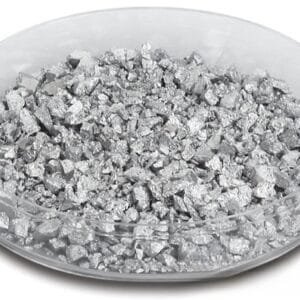
| Appearance/Color | White solid |
| Melting Point | 1,490 °C (2,710 °F; 1,760 K) |
| Density | 4.91 g/cm3 |
| Purity | 99.5% |
| Shape | Powder/ Granule/ Custom-made |
Applications
Chromium disilicide evaporation materials are widely used in:
- Semiconductor Deposition
- Chemical Vapor Deposition (CVD)
- Physical Vapor Deposition (PVD)
These materials are especially useful in optics applications such as wear-resistant coatings, decorative finishes, and display technologies.
Packaging and Handling
Our chromium(II) silicide materials are meticulously tagged and labeled for clear identification and effective quality control. We take great care to prevent damage during storage and transportation to ensure the materials arrive in excellent condition.
Contact Us
TFM is a leading provider of high-purity chromium(II) silicide evaporation materials, available in various forms including tablets, granules, rods, and wires. Customized shapes and quantities are also offered to meet specific needs. Additionally, we supply evaporation sources, boats, filaments, crucibles, heaters, and e-beam crucible liners. For current pricing or inquiries about other materials, please contact us directly.


Reviews
There are no reviews yet.