
Chromium Silicide Sputtering Target Description
Chromium Silicide Sputtering Targets are essential materials for thin film deposition in various applications. Comprising chromium (Cr) and silicon (Si), these targets offer unique properties crucial for both electronic and optical uses. They enable the deposition of thin films with high electrical conductivity, thermal stability, and corrosion resistance. Chromium Silicide films are widely used in semiconductor manufacturing, solar cells, sensors, and magnetic storage devices. By providing precise control over film thickness and composition, Chromium Silicide Sputtering Targets support the creation of advanced electronic and optoelectronic components across numerous industrial and research applications.
Related Product: Chromium Sputtering Target, Chromium Cobalt Sputtering Target
Chromium Silicide Sputtering Target Specifications
| Compound Formula | Cr3Si |
| Molecular Weight | 184.07 |
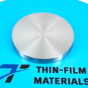
| Appearance | Silver Grey Target |
| Available Sizes | Dia.: 1.0″, 2.0″, 3.0″, 4.0″, 5.0″, 6.0″ Thick: 0.125″, 0.250″ |
Chromium Silicide Sputtering Target Handling Notes
Chromium Silicide Sputtering Target Application
Chromium Silicide Sputtering Target Packaging
Get Contact
TFM offers Chromium Silicide Sputtering Targets in various forms, purities, sizes, and prices. We specialize in high-purity thin film deposition materials with optimal density and minimal grain sizes, which are ideal for semiconductor, CVD, and PVD applications in display and optics. Contact Us for current pricing on sputtering targets and other deposition materials that are not listed.


Reviews
There are no reviews yet.