
 MSDS File
Introduction
Chromium(III) Sulfide (Cr₂S₃) Evaporation Materials are specialized source materials used in vacuum thin-film deposition for functional, protective, and electronic coatings. As a transition-metal sulfide, Cr₂S₃ is valued for its chemical stability, wear resistance, and unique electrical and optical characteristics, making it suitable for both applied research and advanced industrial coating processes.
Detailed Description
Our Chromium(III) Sulfide Evaporation Materials are synthesized from high-purity chromium and sulfur under carefully controlled conditions to ensure accurate stoichiometry and phase stability. Maintaining the correct Cr:S ratio is critical, as deviations can affect film conductivity, structural integrity, and long-term performance.
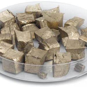
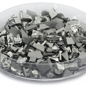
The material is supplied in evaporation-ready forms such as pellets, pieces, or granules, optimized for stable thermal or electron-beam evaporation. Controlled particle size and density help achieve smooth evaporation behavior, minimizing spitting and compositional fluctuation during deposition. High purity levels reduce the presence of oxygen and metallic contaminants, resulting in dense, uniform films with reproducible properties.
Cr₂S₃ evaporation materials are compatible with high-vacuum (HV) and ultra-high-vacuum (UHV) systems. They can be used in single-source evaporation or integrated into multilayer coating designs where chromium sulfide layers provide functional or protective performance. Custom sizing, purity grades, and packaging options are available to match specific evaporation sources and process requirements.
Applications
Chromium(III) Sulfide Evaporation Materials are commonly used in:
Wear-resistant and protective thin-film coatings
Functional sulfide layers in electronic and sensor devices
Optical and infrared-related thin films
Tribological and corrosion-resistant coatings
Academic and industrial R&D on transition-metal sulfides
They are particularly suitable for applications requiring stable sulfide phases and controlled film composition.
Technical Parameters
| Parameter | Typical Value / Range | Importance |
|---|---|---|
| Chemical Formula | Cr₂S₃ | Defines material phase and film properties |
| Purity | 99.9% – 99.99% | Reduces impurities affecting film quality |
| Form | Pellets / Pieces / Granules | Compatible with various evaporation sources |
| Deposition Method | Thermal / E-beam evaporation | Supports standard vacuum processes |
| Vacuum Compatibility | HV / UHV | Ensures low contamination during deposition |
| Packaging | Vacuum-sealed | Protects against oxidation and moisture |
Comparison with Related Materials
| Material | Key Advantage | Typical Application |
|---|---|---|
| Chromium(III) Sulfide (Cr₂S₃) | Chemical stability, wear resistance | Functional & protective coatings |
| Chromium Metal | High hardness, conductivity | Metallic and barrier layers |
| Molybdenum Disulfide (MoS₂) | Solid lubrication | Low-friction coatings |
FAQ
| Question | Answer |
|---|---|
| Can Cr₂S₃ be used for e-beam evaporation? | Yes, it is suitable for both thermal and e-beam evaporation when properly conditioned. |
| Are different particle sizes available? | Yes, particle size and form can be customized for specific crucibles or sources. |
| How is stoichiometry controlled? | Controlled synthesis and batch testing ensure consistent Cr₂S₃ composition. |
| Do you supply small research quantities? | Yes, both small R&D and bulk quantities are available. |
Packaging
Our Chromium(III) Sulfide Evaporation Materials are carefully vacuum-sealed, clearly labeled, and packed with protective materials to maintain chemical integrity and prevent contamination during storage and transportation.
Conclusion
Chromium(III) Sulfide (Cr₂S₃) Evaporation Materials offer a reliable, high-purity solution for depositing stable sulfide thin films with functional and protective properties. With controlled stoichiometry, flexible material forms, and compatibility with standard vacuum evaporation techniques, they are well suited for demanding research and industrial applications.
For detailed specifications and a quotation, please contact us at sales@thinfilmmaterials.com.

Reviews
There are no reviews yet.