

Introduction
Copper Indium sputtering targets are widely used in advanced thin-film deposition processes, particularly in applications where precise control of electrical, optical, and compositional properties is required. As a key precursor material for copper–indium–based functional layers, Cu/In targets play an important role in semiconductor research, optoelectronic devices, and energy-related thin films, offering excellent compatibility with modern PVD sputtering systems.
Detailed Description
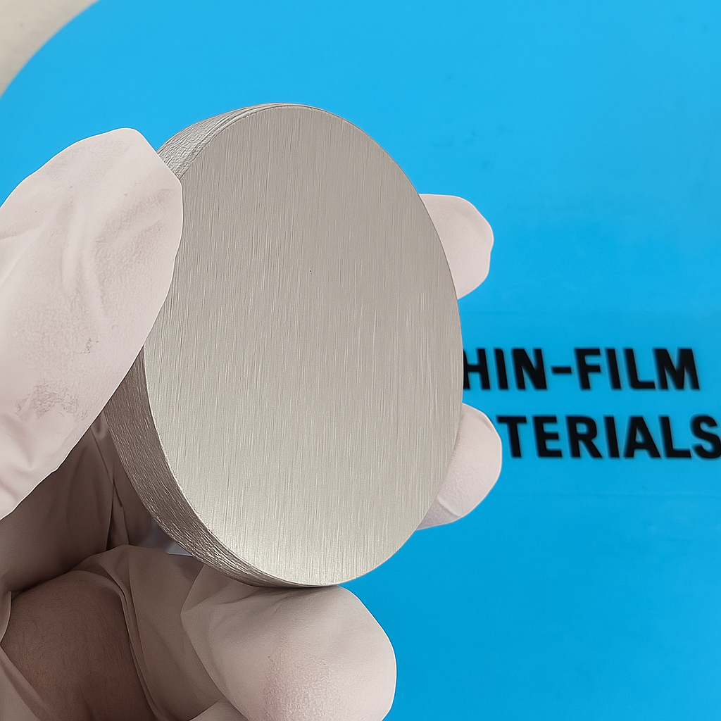
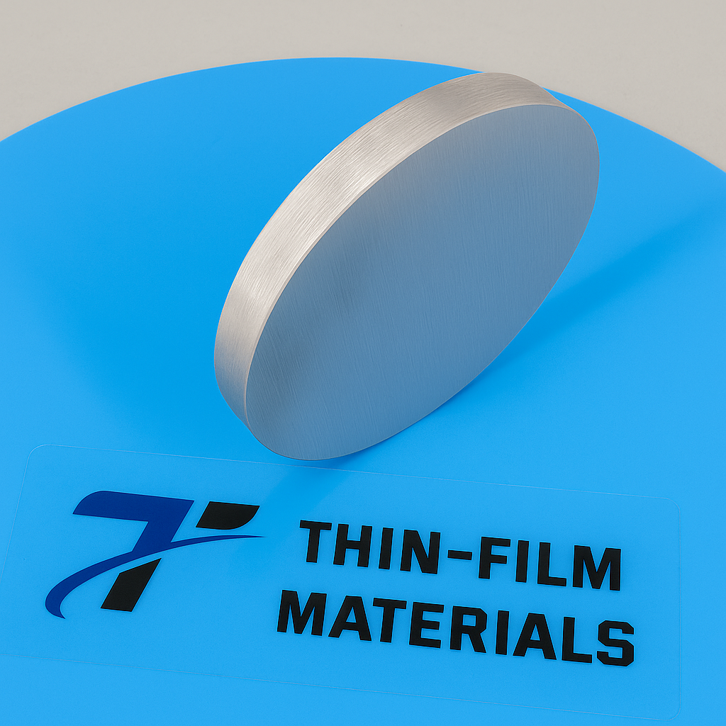
The Copper Indium Sputtering Target (Cu/In) is typically manufactured as a composite or alloy target, depending on the required stoichiometry and deposition process. By carefully controlling the copper-to-indium ratio, the target enables consistent transfer of material composition from target to substrate, which is critical for achieving uniform film properties.
Copper contributes high electrical conductivity and structural stability, while indium provides excellent ductility and favorable electronic characteristics. The combination allows Cu/In targets to support smooth sputtering behavior, reduced particle generation, and stable plasma conditions. Targets can be produced with high density through advanced powder metallurgy or vacuum hot-pressing techniques, improving sputtering efficiency and extending target lifetime.
Available in a wide range of diameters and thicknesses, Copper Indium sputtering targets can be supplied as unbonded discs or bonded to copper or titanium backing plates. Proper bonding enhances heat dissipation during sputtering, minimizes thermal stress, and ensures reliable performance in both DC and RF sputtering systems.
Applications
Copper Indium Sputtering Targets are commonly used in the following fields:
Thin film deposition for semiconductor and microelectronic devices
Photovoltaic research, including precursor layers for CIGS-based solar cells
Transparent and conductive thin films for optoelectronics
Functional coatings in sensors and electronic components
R&D applications requiring precise composition control
Technical Parameters
| Parameter | Typical Value / Range | Importance |
|---|---|---|
| Composition | Cu/In (custom atomic or weight ratio) | Determines film stoichiometry |
| Purity | 99.9% – 99.99% | Reduces impurities and defects in films |
| Diameter | 25 – 300 mm (custom) | Compatible with various sputtering systems |
| Thickness | 3 – 6 mm (custom available) | Influences sputtering rate and lifetime |
| Density | ≥99% of theoretical | Ensures stable and uniform sputtering |
| Bonding | Copper or Titanium backing | Improves heat transfer and stability |
Comparison with Related Materials
| Material | Key Advantage | Typical Application |
|---|---|---|
| Copper Indium Sputtering Target | Precise Cu/In ratio control | Semiconductor & photovoltaic films |
| Copper Sputtering Target | High conductivity | Interconnect and conductive layers |
| Indium Sputtering Target | Excellent ductility | Transparent conductive coatings |
FAQ
| Question | Answer |
|---|---|
| Can the Cu/In ratio be customized? | Yes, the composition can be tailored to specific atomic or weight ratios. |
| Is bonding to a backing plate required? | Bonding is optional but recommended for better thermal management. |
| Which sputtering methods are suitable? | Compatible with DC and RF sputtering systems. |
| How is the target packaged? | Vacuum-sealed with protective materials in export-grade cartons or crates. |
Packaging
Our Copper Indium Sputtering Targets are meticulously tagged and labeled externally to ensure efficient identification and strict quality control. Each target is carefully protected against mechanical damage and contamination during storage and transportation, ensuring it arrives in optimal condition for immediate use.
Conclusion
Copper Indium Sputtering Targets provide a reliable and flexible solution for high-performance thin-film deposition, combining the advantages of copper and indium in a single, customizable material system. With consistent quality, precise composition control, and tailored manufacturing options, these targets are well suited for both industrial production and advanced research applications.
For detailed specifications and a quotation, please contact us at sales@thinfilmmaterials.com.


Reviews
There are no reviews yet.