 MSDS File
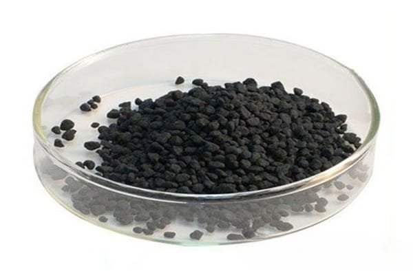
Copper monosulfide (CuS) is a specialized sulfide ceramic evaporation material essential for high-quality deposition processes. Known for its superior performance, CuS is used in creating thin films with exceptional reliability. TFM ensures the highest purity levels, up to 99.9995%, through stringent quality control measures.
Copper Monosulfide Evaporation Materials Specification
| Material Type | Copper monosulfide |
| Symbol | CuS |
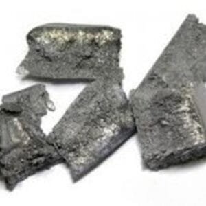
| Appearance/Color | Black solid |
| Melting Point | Above 500 °C (932 °F; 773 K) (decomposes) |
| Density | 4.76 g/cm3 |
| Purity | 99.9% ~ 99.95% |
| Shape | Powder/ Granule/ Custom-made |
Applications
Copper monosulfide evaporation materials are utilized in various deposition techniques, including:
- Semiconductor Deposition
- Chemical Vapor Deposition (CVD)
- Physical Vapor Deposition (PVD)
These materials are ideal for optical applications such as wear protection, decorative coatings, and displays.
Packaging
Copper monosulfide evaporation materials are carefully tagged and labeled to ensure efficient identification and quality control. The packaging is designed to prevent damage during storage and transportation.
Contact Us
TFM is a leading supplier of high-purity copper monosulfide evaporation materials, offering them in various forms such as tablets, granules, rods, and wires. Custom shapes and quantities are available upon request. We also provide related products including evaporation sources, boats, filaments, crucibles, heaters, and e-beam crucible liners. For current prices and additional information, please send us an inquiry.


Reviews
There are no reviews yet.