Generic selectors
Exact matches only
Search in title
Search in content
Post Type Selectors

ST0011 Copper Sputtering Target, Cu

Chemical Formula: Cu
Catalog Number: ST0011
CAS Number: 7440-50-8
Purity: 99.9%, 99.99%, 99.999%
Shape: Discs, Plates, Column Targets, Step Targets, Custom-made

Copper sputtering target  come in various forms, purities, sizes, and prices. Thin Film Materials (TFM) manufactures and supplies top-quality sputtering targets at competitive prices.

MSDS File

Availability: 1 in stock

$22.00

Product Overview

Copper

Copper, symbolized as Cu, is a highly versatile element known for its excellent electrical and thermal conductivity, corrosion resistance, and malleability. Our Copper Sputtering Targets, made from high-purity copper, retain these properties, making them perfect for a wide range of deposition applications.

Key Features

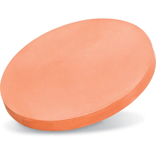
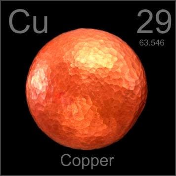
  • Material Type: Pure Copper (Cu)
  • Color/Appearance: Metallic, Copper
  • Melting Point: 1,083°C
  • Density: 8.96 g/cm³
  • Sputter: DC
  • Bonding Types Available: Indium, Elastomer
  • Available Sizes: Diameters from 2.0″ to 6.0″, Thicknesses from 0.125″ to 0.250″

Advanced Specifications

Purity Levels: Our high-purity copper starts at 99.99%, ensuring superior performance in your sputtering processes.

Customization: We offer customized shapes and sizes to meet the specific needs of your applications. Contact us to discuss your requirements.

Applications

Copper sputtering targets are essential in various high-tech applications:

  • Semiconductor Manufacturing: Crucial for producing semiconductors where high-purity copper ensures reliable and efficient devices.
  • Thin Film Deposition: Ideal for creating conductive layers in thin-film transistors (TFTs) used in large-format, high-resolution displays.
  • Photovoltaic Devices: Used in the deposition processes for solar cells, enhancing their efficiency and performance.
  • Optical Storage Media: Essential for producing recording layers in CD-ROMs and other optical storage devices.

Planar and Rotary Targets

Planar Targets: Our planar copper targets feature high density and uniform grain structures, ensuring consistent performance and long target life.

Rotary Targets: Designed for high utilization rates, our rotary copper targets reduce material waste and enhance the efficiency of your sputtering operations.

Bonding and Backing Services

Specialized bonding services for Copper Sputtering Targets, including indium and elastomeric bonding techniques, enhance performance and durability. Thin Film Materials (TFM) ensures high-quality solutions that meet industry standards and customer needs.

We also offer custom machining of backing plates, which is essential for sputtering target assembly. This comprehensive approach improves target design flexibility and performance in thin film deposition. Our channels provide detailed information about bonding materials, methods, and services, helping clients make informed decisions.

Quality Assurance and Packaging

Our Copper Sputtering Targets are clearly tagged and labeled externally to ensure efficient identification and quality control. We take great care to prevent any damage during storage and transportation.

Contact Us

TFM offers Copper Sputtering Targets in various forms, purities, sizes, and prices. We specialize in high-purity thin film deposition materials with optimal density and minimal grain sizes, which are ideal for semiconductor, CVD, and PVD applications in display and optics. Contact Us for current pricing on sputtering targets and other deposition materials that are not listed.

Reviews

There are no reviews yet.

Be the first to review “ST0011 Copper Sputtering Target, Cu”

Your email address will not be published. Required fields are marked *

Related Products

FAQ

It’s the source material (in solid form) used in sputter deposition to eject atoms or molecules that then form a thin film on a substrate.

Targets can be pure metals (e.g., gold, copper, aluminum), ceramics (e.g., Al₂O₃, SiO₂, TiO₂), alloys, or composites—chosen based on the film’s desired properties.


They are produced by processes such as melting/casting for metals or sintering (often with hot isostatic pressing) for ceramics and composite targets to ensure high density and purity.


In a vacuum chamber, a plasma (typically argon) bombards the target, ejecting atoms that travel and condense on a substrate, forming a thin film.


Key factors include the target’s purity, density, grain structure, and the sputtering yield (i.e. how many atoms are ejected per incident ion), as well as operating conditions like power density and gas pressure.


Operators monitor target erosion (often by measuring the depth of the eroded “race track”) or track total energy delivered (kilowatt-hours) until it reaches a threshold that can compromise film quality.


Fragile materials (such as many ceramics or certain oxides) and precious metals often require a backing plate to improve cooling, mechanical stability, and to allow thinner targets that reduce material costs.


DC sputtering is used for conductive targets, while RF sputtering is necessary for insulating targets (like many oxides) because it prevents charge buildup on the target’s surface.


In reactive sputtering, a reactive gas (e.g., oxygen or nitrogen) is introduced to form compound films on the substrate, but it may also “poison” the target surface if not carefully controlled.


Many manufacturers prefer to control raw material quality by sourcing their own powders; using external powders can risk impurities and inconsistent target properties.


Targets should be stored in clean, dry conditions (often in original packaging or re-wrapped in protective materials) and handled with gloves to avoid contamination, ensuring optimal performance during deposition.

Deposition rate depends on factors such as target material and composition, power density, working gas pressure, substrate distance, and the configuration of the sputtering system (e.g., magnetron design).

 
Shopping Cart
Scroll to Top