Generic selectors
Exact matches only
Search in title
Search in content
Post Type Selectors

ST0938 Copper (II) Telluride Sputtering Target, CuTe

Chemical Formula CuTe
Catalog No. ST0938
CAS Number 12019-23-7
Purity 99.9%, 99.95%, 99.99%, 99.995%, 99.999%
Shape Discs, Plates, Column Targets, Step Targets, Custom-made

Copper (II) Telluride sputtering target  come in various forms, purities, sizes, and prices. Thin Film Materials (TFM) manufactures and supplies top-quality sputtering targets at competitive prices.

MSDS File

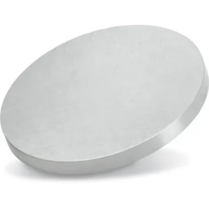
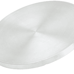
Copper (II) Telluride Sputtering Target Description

Copper (II) Telluride Sputtering Targets, supplied by TFM, are engineered with optimal density and minimal average grain size, making them ideal for applications in the semiconductor, electronics, optics, and photonics industries. These targets are essential in the sputtering process, where high-energy ions bombard the target material, causing atoms or molecules to be ejected and deposited as a thin film onto a substrate.

Copper (II) Telluride (CuTe) is a semiconductor material known for its intermediate electrical conductivity, sitting between that of a conductor and an insulator. Notably, its resistivity decreases as temperature increases, making it a valuable material for temperature-sensitive applications.

Related Product: Copper Sputtering Target, Copper Oxide Sputtering Target

Copper (II) Telluride Sputtering Target Specifications

Compound Formula CuTe
Molecular Weight 191.15
Appearance Black Target
Melting Point 1125℃
Density 7.1 g/cm3
Available Sizes Dia.: 1.0″, 2.0″, 3.0″, 4.0″, 5.0″, 6.0″

Thick: 0.125″, 0.250″

Copper (II) Telluride Sputtering Target Handling Notes

Indium bonding is advised for the Copper (II) Telluride Sputtering Target due to certain characteristics that make it challenging for sputtering, such as brittleness and low thermal conductivity. This material is prone to thermal shock, making the indium bonding process beneficial for enhancing its stability and performance during sputtering.

Copper (II) Telluride Sputtering Target Application

Copper (II) Telluride Sputtering Targets are utilized in electron beam evaporation coating and magnetron sputtering coating, leveraging their high purity, high density, high conductivity, and excellent crystalline properties. These targets are particularly valuable in semiconductor-related fields due to their unique electrical properties.

Additionally, Copper (II) Telluride Sputtering Targets are used to prepare thin films that exhibit high transmittance, high reflectivity, and high conductivity. These characteristics make them ideal for applications in solar cells, optoelectronic devices, and other advanced technologies.

Copper (II) Telluride Sputtering Target Packaging

Our Copper (II) Telluride Sputtering Target is meticulously handled during storage and transportation to ensure that the quality of our products is preserved in their original condition.

Get Contact

TFM offers Copper (II) Telluride Sputtering Targets in various forms, purities, sizes, and prices. We specialize in high-purity thin film deposition materials with optimal density and minimal grain sizes, which are ideal for semiconductor, CVD, and PVD applications in display and optics. Contact Us for current pricing on sputtering targets and other deposition materials that are not listed.

Reviews

There are no reviews yet.

Be the first to review “ST0938 Copper (II) Telluride Sputtering Target, CuTe”

Your email address will not be published. Required fields are marked *

Related Products

FAQ

It’s the source material (in solid form) used in sputter deposition to eject atoms or molecules that then form a thin film on a substrate.

Targets can be pure metals (e.g., gold, copper, aluminum), ceramics (e.g., Al₂O₃, SiO₂, TiO₂), alloys, or composites—chosen based on the film’s desired properties.


They are produced by processes such as melting/casting for metals or sintering (often with hot isostatic pressing) for ceramics and composite targets to ensure high density and purity.


In a vacuum chamber, a plasma (typically argon) bombards the target, ejecting atoms that travel and condense on a substrate, forming a thin film.


Key factors include the target’s purity, density, grain structure, and the sputtering yield (i.e. how many atoms are ejected per incident ion), as well as operating conditions like power density and gas pressure.


Operators monitor target erosion (often by measuring the depth of the eroded “race track”) or track total energy delivered (kilowatt-hours) until it reaches a threshold that can compromise film quality.


Fragile materials (such as many ceramics or certain oxides) and precious metals often require a backing plate to improve cooling, mechanical stability, and to allow thinner targets that reduce material costs.


DC sputtering is used for conductive targets, while RF sputtering is necessary for insulating targets (like many oxides) because it prevents charge buildup on the target’s surface.


In reactive sputtering, a reactive gas (e.g., oxygen or nitrogen) is introduced to form compound films on the substrate, but it may also “poison” the target surface if not carefully controlled.


Many manufacturers prefer to control raw material quality by sourcing their own powders; using external powders can risk impurities and inconsistent target properties.


Targets should be stored in clean, dry conditions (often in original packaging or re-wrapped in protective materials) and handled with gloves to avoid contamination, ensuring optimal performance during deposition.

Deposition rate depends on factors such as target material and composition, power density, working gas pressure, substrate distance, and the configuration of the sputtering system (e.g., magnetron design).

 
Shopping Cart
Scroll to Top