Copper Zirconium Sputtering Target
Introduction
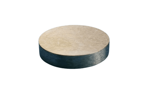
Copper Zirconium (CuZr) Sputtering Target is an alloy material designed for high-performance thin film deposition. By combining copper’s superior electrical and thermal conductivity with zirconium’s grain refinement and strengthening effects, this sputtering target offers stable sputtering behavior, improved durability, and high-quality film formation. It is widely applied in semiconductors, displays, photovoltaic devices, and advanced R&D.
Detailed Description
Copper Zirconium sputtering targets are produced using advanced vacuum melting or powder metallurgy, followed by precision machining to achieve dense, uniform, and crack-free targets.
Composition: Typically Cu with 0.1–1.0 wt% Zr; custom compositions available.
Purity: ≥ 99.9% ensures low contamination and reliable thin film performance.
Microstructure: Fine-grained, homogeneous alloy minimizes arcing and enhances film adhesion.
Dimensions: Available in circular (25–300 mm), rectangular, or custom shapes; thickness 3–6 mm.
Bonding Options: Indium or elastomer bonding to copper or titanium backing plates for improved heat dissipation and mechanical stability.
Applications
Copper Zirconium sputtering targets are used in multiple industries and research fields:
Semiconductors – Conductive and barrier films in microelectronic devices.
Display Technology – Transparent and conductive films for TFT-LCD and OLEDs.
Photovoltaics – Back contact and functional coatings in solar cells.
Decorative Coatings – Corrosion-resistant, durable thin films for consumer goods.
R&D – Alloy thin films for materials science and next-generation electronics.
Technical Parameters
| Parameter | Typical Value / Range | Importance |
|---|---|---|
| Purity | ≥ 99.9% | Ensures stable electrical/optical film properties |
| Diameter | 25 – 300 mm (custom) | Compatible with most sputtering systems |
| Thickness | 3 – 6 mm | Affects sputtering efficiency and deposition rate |
| Bonding | Copper / Titanium backing | Improves thermal transfer and stability |
| Composition (Cu:Zr) | 0.1–1.0 wt% Zr (customizable) | Enhances strength & film adhesion |
Comparison with Related Materials
| Material | Key Advantage | Typical Application |
|---|---|---|
| Copper Zirconium Alloy Target | Conductivity + strength, grain refinement | Semiconductors, photovoltaics |
| Pure Copper Target | Excellent electrical conductivity | Interconnects, wiring films |
| Pure Zirconium Target | High corrosion resistance | Specialty coatings, R&D |
FAQ
| Question | Answer |
|---|---|
| Can the Zr content be adjusted? | Yes, zirconium concentration can be customized to suit application needs. |
| What is the lead time? | Typically 2–3 weeks depending on specifications and quantity. |
| Is backing plate bonding required? | Recommended for large-diameter or high-power sputtering systems. |
| How are targets packaged? | Vacuum-sealed with desiccants, cushioned with foam, and shipped in export-safe cartons or wooden crates. |
| Which industries use CuZr targets most? | Electronics, display technologies, solar energy, and advanced materials research. |
Packaging
Copper Zirconium sputtering targets are vacuum-sealed to prevent oxidation, labeled for traceability, and packed with protective foam in export-grade cartons or wooden crates to ensure safe transport and storage.
Conclusion
Copper Zirconium Sputtering Targets combine the conductivity of copper with the strengthening effect of zirconium, making them ideal for reliable thin film deposition in semiconductors, displays, and photovoltaic applications. With customizable purity, composition, and bonding options, they deliver high performance for both industrial and research applications.
For detailed specifications and a quotation, please contact us at [sales@thinfilmmaterials.com].

Reviews
There are no reviews yet.