
 MSDS File
| Material Type | Copper(I) Telluride |
| Symbol | Cu2Te |
| Color/Appearance | |
| Melting Point (°C) | |
| Theoretical Density (g/cc) |
| Z Ratio | – |
| E-Beam | – |
| Thermal Evaporation Techniques | Boat: – Crucible: – |
| E-Beam Crucible Liner Material | – |
| Temp. (°C) for Given Vap. Press. (Torr) | – |
| Comments | – |
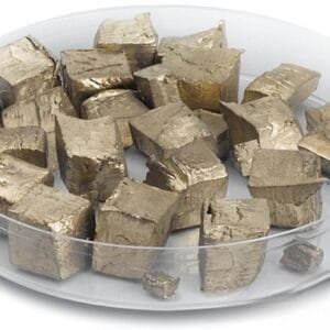
Copper(I) Telluride Pellet Evaporation Material
TFM offers high-purity Copper(I) Telluride (Cu₂Te) Pellet Evaporation Material, widely used in thin-film deposition, optoelectronics, and semiconductor applications. Known for its excellent stability and high electrical conductivity, Cu₂Te is an essential material for infrared detectors, thermoelectric devices, and advanced electronic components.
Key Features and Advantages
High Purity (99.99% – 99.999%): Ensures superior material quality for precise thin-film deposition.
Stable Crystal Structure: Can be stored at room temperature without degradation, ensuring long-term usability.
Excellent Electrical & Optical Properties: Ideal for infrared detection, energy conversion, and semiconductor applications.
Optimized for Thin-Film Deposition: Suitable for thermal evaporation and electron beam (E-beam) evaporation.
Available in Multiple Forms: Offered in pellets, pieces, and powder to meet various research and industrial needs.
Applications
Infrared Detectors & Sensors – Utilized in infrared imaging, night vision, and spectroscopic applications.
Thermoelectric Devices – Plays a key role in energy harvesting and temperature control technologies.
Thin-Film Semiconductor Coatings – Used in optoelectronic components, photovoltaics, and specialty coatings.
Advanced Research & Development – Supports cutting-edge studies in material science and nanotechnology.
Industry Impact
TFM’s Copper(I) Telluride Pellet Evaporation Material is a critical component for semiconductor research, optoelectronic advancements, and infrared applications. With high purity, exceptional stability, and tailored deposition properties, Cu₂Te from TFM ensures consistent and reliable performance for advanced material development and next-generation electronics.


Reviews
There are no reviews yet.