 MSDS File
Introduction
Erbium Evaporation Materials (Er) are high-purity rare earth metal sources used in physical vapor deposition (PVD) processes for optical, semiconductor, and functional thin film applications. Erbium is especially valued for its optical emission at approximately 1.55 µm, a wavelength critical to fiber-optic communications and photonic devices.
In vacuum deposition systems, erbium enables precise rare-earth doping and oxide film formation, supporting the development of advanced optoelectronic components, infrared coatings, and research-grade thin films. Consistent purity and controlled morphology are essential for stable evaporation behavior and reproducible film properties.
Detailed Description
Erbium (Er) is a lanthanide metal with a melting point of approximately 1529 °C and strong affinity for oxygen. It readily forms stable oxides such as Er₂O₃, which are widely used in optical coatings and dielectric layers.
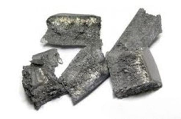
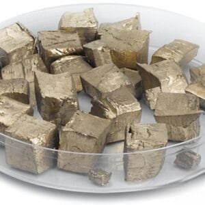
Erbium evaporation materials are typically supplied in:
Small pieces or chunks
Granules
Distilled rods
Custom-cut slugs
High-purity grades (99.9% – 99.99%) are available to minimize contamination in sensitive photonic and semiconductor applications. Low oxygen and metallic impurity levels help ensure optical transparency and controlled film composition.
Due to its melting point, erbium is commonly used in electron beam evaporation systems, although thermal evaporation may be suitable for smaller loads. In reactive deposition environments, oxygen partial pressure must be carefully managed to achieve desired oxide stoichiometry.
Key characteristics include:
Narrow-band infrared optical emission
Strong oxide-forming behavior
Good compatibility with co-evaporation systems
Stable performance in high-vacuum environments
Erbium is frequently incorporated into host materials to create active optical layers for light amplification and signal processing.
Applications
Erbium Evaporation Materials are widely used in:
Optical amplifiers and waveguide devices
Er-doped thin films for photonics research
Infrared optical coatings
High-k dielectric research (Er₂O₃ films)
Semiconductor and advanced oxide deposition
Solid-state laser materials research
Display and functional coating applications
Erbium-doped films are particularly important in optical communication technologies due to their compatibility with standard telecom wavelengths.
Technical Parameters
| Parameter | Typical Value / Range | Importance |
|---|---|---|
| Chemical Symbol | Er | Defines rare-earth optical behavior |
| Purity | 99.9% – 99.99% | Improves film clarity and device performance |
| Form | Pieces / Granules / Rods | Matches evaporation source configuration |
| Melting Point | ~1529 °C | Suitable for e-beam evaporation |
| Density | ~9.07 g/cm³ | Relevant for deposition rate calculations |
| Recommended Method | E-beam / Reactive Evaporation | Ensures stoichiometric control |
Custom sizes and packaging options are available based on deposition system requirements.
Comparison with Related Rare Earth Materials
| Material | Key Advantage | Typical Application |
|---|---|---|
| Erbium (Er) | 1.55 µm optical emission | Fiber-optic & photonic devices |
| Ytterbium (Yb) | High laser efficiency | High-power solid-state lasers |
| Thulium (Tm) | Mid-IR emission range | Infrared photonics |
| Neodymium (Nd) | Strong visible/near-IR emission | Nd:YAG laser systems |
Compared to other rare-earth elements, erbium is uniquely suited for telecommunications and integrated photonics due to its emission wavelength compatibility.
FAQ
| Question | Answer |
|---|---|
| Is erbium suitable for thermal evaporation? | It can be used, but electron beam evaporation is generally preferred for stability. |
| Can it be used for oxide film deposition? | Yes, reactive evaporation can produce Er₂O₃ thin films. |
| Does it require special storage? | Yes, store in a dry or inert environment to minimize surface oxidation. |
| Is it compatible with co-evaporation systems? | Yes, it is often co-evaporated with host materials for doped films. |
| Are certificates provided? | Yes, chemical analysis and batch traceability documentation are available. |
Packaging
Our Erbium Evaporation Materials are meticulously tagged and labeled externally to ensure efficient identification and maintain high standards of quality control. Materials are typically vacuum-sealed or packed under inert gas to prevent oxidation during storage and transport, ensuring they arrive in optimal condition.
Conclusion
Erbium Evaporation Materials (Er) provide a reliable solution for photonic, infrared, and functional oxide thin film applications. With controlled purity, stable evaporation performance, and customizable forms, they support advanced research and industrial thin film production.
For detailed specifications and a quotation, please contact us at sales@thinfilmmaterials.com.
Ordering Table
| Material | Size | Quantity | Purity | Part Number |
| Erbium | < 5mm | 300 g | 99.9% | EVMERX3MM-L |
| Erbium | < 5mm | 100 g | 99.9% | EVMERX5MM-D |


Reviews
There are no reviews yet.