
Introduction
Erbium Fluoride Sputtering Target (ErF₃) is a specialized rare-earth compound target used in thin film deposition processes where low optical loss, chemical stability, and precise refractive index control are required. As a fluoride-based sputtering material, ErF₃ plays an important role in advanced optical coatings, photonic devices, and functional thin films, particularly in applications sensitive to oxygen contamination or requiring fluorine-rich compositions.
Detailed Description
Erbium Fluoride (ErF₃) sputtering targets are typically manufactured from high-purity erbium fluoride powder using controlled pressing and sintering techniques to achieve uniform density and stable sputtering behavior. Compared with oxide-based erbium targets, ErF₃ enables the direct deposition of fluoride films without introducing oxygen, which is critical for maintaining optical transparency in the infrared and minimizing absorption losses.
The intrinsic properties of ErF₃—such as its wide bandgap, low phonon energy, and chemical inertness—make it suitable for optical and photonic thin films. During sputtering, ErF₃ targets exhibit relatively stable erosion profiles and reduced target poisoning risks compared to reactive sputtering routes. This contributes to better film composition control and improved process repeatability.
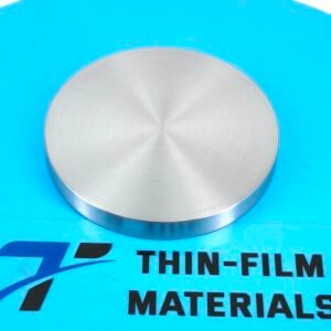
Targets can be supplied in monolithic form or bonded to backing plates (such as copper or titanium) to enhance thermal dissipation and mechanical stability during sputtering. Target dimensions, thickness, and bonding methods are customizable to match various magnetron sputtering systems.
Applications
Erbium Fluoride Sputtering Targets are commonly used in:
Optical and infrared (IR) thin film coatings
Anti-reflective and protective optical layers
Photonic and laser-related components
Fluoride-based dielectric films
Display and optoelectronic devices
Research and development of rare-earth fluoride materials
Technical Parameters
| Parameter | Typical Value / Range | Importance |
|---|---|---|
| Chemical Formula | ErF₃ | Defines fluoride-based film composition |
| Purity | 99.9% – 99.99% | Reduces optical loss and impurities |
| Form | Disc, plate, custom shapes | Compatible with various sputtering systems |
| Diameter | 25 – 300 mm (custom) | Matches magnetron cathode sizes |
| Thickness | 3 – 6 mm (typical) | Influences sputtering rate and lifetime |
| Backing Plate | Copper / Titanium (optional) | Improves heat transfer and stability |
| Density | ≥ 95% of theoretical | Ensures uniform sputtering performance |
Comparison with Related Erbium Materials
| Material | Key Advantage | Typical Application |
|---|---|---|
| Erbium Fluoride (ErF₃) | Oxygen-free fluoride films | Optical & IR coatings |
| Erbium Oxide (Er₂O₃) | High chemical stability | General dielectric coatings |
| Metallic Erbium | Conductive films | Specialty electronic layers |
FAQ
| Question | Answer |
|---|---|
| Why choose ErF₃ instead of Er₂O₃? | ErF₃ enables direct deposition of fluoride films without oxygen incorporation. |
| Can the target be bonded to a backing plate? | Yes, copper or titanium backing plates are available. |
| Is ErF₃ suitable for RF sputtering? | Yes, RF sputtering is commonly used for fluoride compound targets. |
| Can the target size be customized? | Yes, diameter, thickness, and shape can be tailored. |
| How is the target packaged? | Vacuum-sealed with protective cushioning for safe transport. |
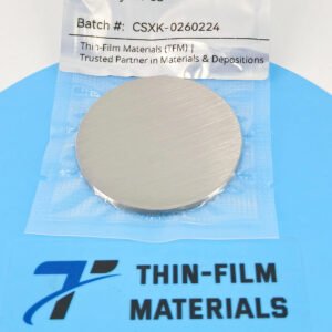
Packaging
Our Erbium Fluoride Sputtering Targets are carefully cleaned, vacuum-sealed, and securely packaged to prevent moisture uptake and contamination. Each target is clearly labeled to ensure traceability and efficient quality control during storage and transportation.
Conclusion
Erbium Fluoride Sputtering Target (ErF₃) offers a reliable solution for depositing high-quality fluoride thin films with excellent optical performance and compositional control. With high purity, customizable dimensions, and optional backing plates, ErF₃ targets are well suited for advanced optical, photonic, and research-driven sputtering applications.
For detailed specifications and a quotation, please contact us at sales@thinfilmmaterials.com.
Reviews
There are no reviews yet.