Generic selectors
Exact matches only
Search in title
Search in content
Post Type Selectors

ST0013 Erbium Sputtering Target, Er

Chemical Formula: Er
Catalog Number: ST0013
CAS Number: 7440-52-0
Purity: 99.9%
Shape: Discs, Plates, Column Targets, Step Targets, Custom-made

Erbium sputtering target  come in various forms, purities, sizes, and prices. Thin Film Materials (TFM) manufactures and supplies top-quality sputtering targets at competitive prices.

MSDS File

Availability: 1 in stock

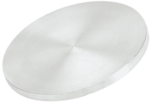
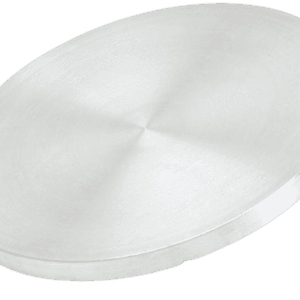
Erbium Sputtering Target Description

Erbium

The erbium sputtering target is composed of high-purity erbium metal. Erbium, symbolized as “Er,” originates from Ytterby, Sweden, and was first identified by G. Mosander in 1842. It has an atomic number of 68, located in Period 6, Group 3 of the periodic table, within the f-block. The relative atomic mass of erbium is 167.259(3) Dalton, with the number in brackets indicating the uncertainty.

Erbium Sputtering Target Specification
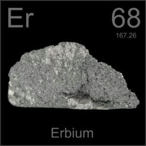
Material Type Erbium
Symbol Er
Color/Appearance Silvery White, Metallic
Melting Point 1,412 °C
Thermal Conductivity 15 W/m.K
Density 9.05 g/cc
Sputter DC
Coefficient of Thermal Expansion 12.2 x 10⁻⁶/K
Available Sizes Dia.: 2.0″, 3.0″, 4.0″, 5.0″, 6.0″
Thick: 0.125″, 0.250″

We also offer other customized shapes and sizes of the sputtering targets; please Contact Us for more information.

Erbium Sputtering Target Application

The erbium sputtering target is used for thin film deposition. Erbium is employed in metallurgical and nuclear sectors; adding erbium to vanadium reduces hardness and enhances workability. Pure erbium is used as an alloying element with titanium and for making infrared absorbing glass. In the ceramics sector, erbium oxide creates a pink glaze. Erbium salts, known for their attractive pastel color, are used as colorants in porcelain enamel glazes and glasses.

Handling Notes

  • Bonding services for erbium sputtering targets are currently unavailable.
  • Due to its high chemical reactivity, erbium sputtering targets require oil packaging and thorough cleaning to prevent environmental reactions.

Packaging

Our Erbium Sputtering Targets are clearly tagged and labeled externally to ensure efficient identification and quality control. We take great care to prevent any damage during storage and transportation.

Get Contact

TFM offers Erbium Sputtering Targets in various forms, purities, sizes, and prices. We specialize in high-purity thin film deposition materials with optimal density and minimal grain sizes, which are ideal for semiconductor, CVD, and PVD applications in display and optics. Contact Us for current pricing on sputtering targets and other deposition materials that are not listed.

Reviews

There are no reviews yet.

Be the first to review “ST0013 Erbium Sputtering Target, Er”

Your email address will not be published. Required fields are marked *

Related Products

FAQ

It’s the source material (in solid form) used in sputter deposition to eject atoms or molecules that then form a thin film on a substrate.

Targets can be pure metals (e.g., gold, copper, aluminum), ceramics (e.g., Al₂O₃, SiO₂, TiO₂), alloys, or composites—chosen based on the film’s desired properties.


They are produced by processes such as melting/casting for metals or sintering (often with hot isostatic pressing) for ceramics and composite targets to ensure high density and purity.


In a vacuum chamber, a plasma (typically argon) bombards the target, ejecting atoms that travel and condense on a substrate, forming a thin film.


Key factors include the target’s purity, density, grain structure, and the sputtering yield (i.e. how many atoms are ejected per incident ion), as well as operating conditions like power density and gas pressure.


Operators monitor target erosion (often by measuring the depth of the eroded “race track”) or track total energy delivered (kilowatt-hours) until it reaches a threshold that can compromise film quality.


Fragile materials (such as many ceramics or certain oxides) and precious metals often require a backing plate to improve cooling, mechanical stability, and to allow thinner targets that reduce material costs.


DC sputtering is used for conductive targets, while RF sputtering is necessary for insulating targets (like many oxides) because it prevents charge buildup on the target’s surface.


In reactive sputtering, a reactive gas (e.g., oxygen or nitrogen) is introduced to form compound films on the substrate, but it may also “poison” the target surface if not carefully controlled.


Many manufacturers prefer to control raw material quality by sourcing their own powders; using external powders can risk impurities and inconsistent target properties.


Targets should be stored in clean, dry conditions (often in original packaging or re-wrapped in protective materials) and handled with gloves to avoid contamination, ensuring optimal performance during deposition.

Deposition rate depends on factors such as target material and composition, power density, working gas pressure, substrate distance, and the configuration of the sputtering system (e.g., magnetron design).

 
Shopping Cart
Scroll to Top