
 MSDS File
| Material Type | Gallium Antimony |
| Symbol | GaSb |
| Melting Point (°C) | 710 |
| Theoretical Density (g/cc) | 5.6 |
| Z Ratio | |
| E-Beam | Fair |
| E-Beam Crucible Liner Material | |
| Temp. (°C) for Given Vap. Press. (Torr) | |
| Comments | Flash evaporate |
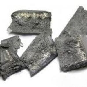
Gallium Antimony Pellet Evaporation Material
TFM offers high-purity Gallium Antimony Pellet Evaporation Material, designed for thin-film deposition in semiconductor, optoelectronic, and infrared applications. Composed of gallium (Ga) and antimony (Sb), gallium antimonide (GaSb) is a narrow-bandgap semiconductor with excellent electronic and optical properties, making it ideal for infrared photodetectors, thermophotovoltaic devices, and high-speed electronic components.
Optimized for thermal evaporation and electron beam (E-beam) deposition, this material ensures uniform film thickness, high purity, and excellent adhesion, supporting advanced research and industrial applications.
Key Features and Advantages
Narrow Bandgap Semiconductor: Gallium antimonide features a small bandgap (~0.72 eV), making it suitable for infrared photodetection, optoelectronic devices, and high-speed transistors.
Superior Infrared Absorption: Ideal for mid- and long-wavelength infrared (MWIR/LWIR) applications, enhancing thermal imaging and optical sensing.
High Electron Mobility: Enables fast electronic switching, supporting high-frequency applications and semiconductor research.
High Purity & Precise Deposition: Guarantees defect-free, uniform thin-film coatings, improving device performance and reliability.
Customizable Composition: TFM provides tailored specifications to meet specific research and industrial requirements.
Applications
Infrared Detectors & Sensors: Used in thermal imaging, night vision systems, and spectroscopy for defense, medical, and industrial applications.
Optoelectronics & Photonics: Applied in infrared LEDs, laser diodes, and optical modulators for telecommunications and sensing technologies.
Thermophotovoltaic (TPV) Devices: Enhances energy conversion efficiency in infrared power generation and renewable energy systems.
High-Speed Electronics: Plays a key role in high-frequency transistors, integrated circuits (ICs), and next-generation semiconductor devices.
Thin-Film Deposition: Ensures high-quality coatings for infrared optics, semiconductor components, and photonic applications.
Industry Impact and Customization
TFM’s Gallium Antimony Pellet Evaporation Material is a crucial material in infrared detection, high-speed optoelectronics, and advanced semiconductor research. With high purity, precise deposition control, and customizable formulations, TFM ensures its materials meet the demands of cutting-edge applications in defense, aerospace, and photonic industries.
By offering exceptional semiconductor properties, infrared absorption, and high-speed electronic capabilities, Gallium Antimony Pellet Evaporation Material from TFM is essential for developing next-generation infrared sensors, efficient thermophotovoltaic systems, and advanced optoelectronic devices.


Reviews
There are no reviews yet.