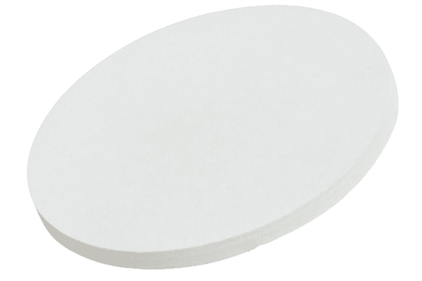
Gallium Oxide–Magnesium Oxide Sputtering Target (Ga₂O₃–MgO)
Introduction
The Gallium Oxide–Magnesium Oxide (Ga₂O₃–MgO) Sputtering Target is a composite oxide material designed for advanced thin film applications requiring excellent optical transparency, wide bandgap, and superior chemical stability. By combining gallium oxide (Ga₂O₃) and magnesium oxide (MgO), this sputtering target enables the formation of high-quality, transparent conductive or insulating films with enhanced mechanical and thermal stability. It is widely used in semiconductor, optoelectronic, and power device manufacturing.
Detailed Description
Gallium oxide is a wide-bandgap semiconductor with exceptional optical and electrical characteristics, while magnesium oxide contributes excellent hardness, high melting point, and chemical durability. The combination of these oxides in a controlled ratio results in films with improved dielectric properties, enhanced thermal stability, and tunable electrical conductivity.
The Ga₂O₃–MgO sputtering target is typically prepared through high-temperature solid-state synthesis, followed by hot pressing or vacuum sintering to achieve high density and uniform phase distribution. This process minimizes porosity and ensures stable sputtering behavior, producing thin films with excellent adhesion and uniform thickness.
Key Features:
High optical transparency in UV–visible–IR range.
Wide bandgap (>4.8 eV) suitable for power and optoelectronic devices.
Excellent film uniformity and low particle generation.
Enhanced chemical and thermal stability due to MgO addition.
Customizable Ga₂O₃:MgO ratios to tailor dielectric and conductivity properties.
Applications
The Ga₂O₃–MgO sputtering target is widely used in:
Semiconductor devices – dielectric layers and transparent conductive films.
Power electronics – wide-bandgap oxide layers for high-voltage components.
Optoelectronic coatings – UV detectors, LEDs, and laser diodes.
Transparent electronics – oxide-based transistors and display backplanes.
Research & development – functional oxide and heterostructure studies.
Technical Parameters
| Parameter | Typical Value / Range | Importance |
|---|---|---|
| Chemical Formula | (Ga₂O₃)₁₋ₓ(MgO)ₓ | Defines composition and performance |
| Purity | 99.9% – 99.99% | Ensures low contamination |
| Density | ≥ 95% theoretical | Improves film uniformity and deposition rate |
| Diameter | 25 – 300 mm (custom) | Compatible with various sputtering systems |
| Thickness | 3 – 10 mm | Balances sputtering stability and target lifespan |
| Backing Plate | Copper / Titanium | Enhances heat dissipation and bonding reliability |
Comparison with Related Materials
| Material | Key Advantage | Typical Application |
|---|---|---|
| Ga₂O₃–MgO | High thermal stability & tunable conductivity | Power & optoelectronic films |
| Ga₂O₃ (Gallium Oxide) | Ultra-wide bandgap & transparency | UV devices, semiconductors |
| MgO (Magnesium Oxide) | Excellent insulation & hardness | Protective coatings |
| ZnO–MgO | Tunable optical bandgap | Transparent semiconductors |
FAQ
| Question | Answer |
|---|---|
| Can Ga₂O₃–MgO targets be customized? | Yes, Ga₂O₃:MgO ratios, sizes, and bonding options can be customized. |
| What bonding options are available? | Copper or titanium backing plates are common. |
| Is the target suitable for RF sputtering? | Yes, ideal for both RF and DC magnetron sputtering systems. |
| How are the targets packaged? | Vacuum-sealed with desiccant, foam-cushioned, and shipped in wooden crates. |
| Which industries use this material most? | Semiconductor, optoelectronic, and power device industries. |
Packaging
Each Gallium Oxide–Magnesium Oxide Sputtering Target is precisely vacuum-sealed in an inert atmosphere to prevent contamination and moisture absorption. Targets are labeled for traceability and securely packed in foam-lined, export-grade cartons or wooden boxes.
Conclusion
The Ga₂O₃–MgO sputtering target combines the superior optical and electronic properties of gallium oxide with the thermal and structural stability of magnesium oxide, offering a robust material for next-generation thin film technologies. Its wide bandgap, high purity, and customizable composition make it a preferred choice for high-performance electronic and optoelectronic coatings.
For detailed specifications and quotations, please contact us at [sales@thinfilmmaterials.com].


Reviews
There are no reviews yet.