Introduction
Germanium Antimony Selenium Tellurium sputtering targets are multicomponent chalcogenide materials engineered for advanced thin-film deposition, particularly in phase-change memory (PCM), optoelectronics, and infrared-related research. By carefully balancing Ge–Sb–Se–Te composition, these targets enable precise tuning of optical contrast, electrical switching behavior, and thermal stability—key requirements for next-generation data storage and functional thin films.
Detailed Description
Ge–Sb–Se–Te (often abbreviated as GSTSe) belongs to the chalcogenide alloy family, where germanium and antimony form the structural backbone while selenium and tellurium tailor crystallization kinetics, bandgap, and optical response. Compared with traditional Ge–Sb–Te systems, selenium incorporation can improve thermal stability, reduce power consumption, and enhance endurance in phase-change applications.
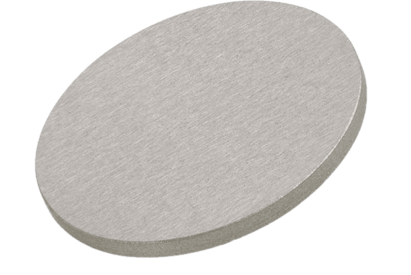
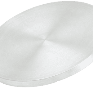
Our Germanium Antimony Selenium Tellurium sputtering targets are fabricated from high-purity elemental precursors using controlled vacuum melting, alloy homogenization, and precision machining. Strict stoichiometric control ensures excellent compositional uniformity across the target, which is essential for repeatable sputtering rates and consistent thin-film properties.
These targets are compatible with DC magnetron sputtering and RF sputtering (depending on composition and system configuration). Planar disc targets are available in standard sizes, with optional indium or elastomer bonding to copper backing plates to improve thermal management and mechanical stability during deposition. Custom compositions and dimensions can be provided to support both research and pilot-scale production.
Applications
Germanium Antimony Selenium Tellurium sputtering targets are commonly used in:
Phase-change memory (PCM) and neuromorphic devices
Non-volatile memory and data storage research
Infrared and optical functional thin films
Chalcogenide semiconductor thin-film studies
Reconfigurable photonic and optical switching devices
Academic and industrial R&D on multicomponent chalcogenides
Technical Parameters
| Parameter | Typical Value / Range | Importance |
|---|---|---|
| Material | Ge–Sb–Se–Te alloy | Defines phase-change & optical behavior |
| Purity | 99.9% – 99.99% | Minimizes defect-induced variability |
| Composition | Custom Ge/Sb/Se/Te ratios | Tunes switching & thermal properties |
| Diameter | 1″ – 4″ (custom available) | Fits standard sputtering cathodes |
| Thickness | 3 – 6 mm | Determines target lifetime |
| Density | High, alloy-controlled | Ensures stable sputtering rate |
| Backing Plate | Optional Cu (bonded) | Improves heat dissipation |
Comparison with Related Materials
| Material | Key Advantage | Typical Application |
|---|---|---|
| Ge–Sb–Se–Te | Improved thermal stability, tunable switching | PCM, photonics |
| Ge–Sb–Te (GST) | Mature PCM material | Data storage |
| Ge–Se | Wide bandgap chalcogenide | Optical films |
| Sb–Te | Fast phase change | Memory research |
FAQ
| Question | Answer |
|---|---|
| Can the alloy composition be customized? | Yes, Ge/Sb/Se/Te ratios can be tailored to your application. |
| Is the target suitable for DC sputtering? | Yes, most compositions are compatible with DC magnetron sputtering. |
| Are bonded targets available? | Yes, indium-bonded or elastomer-bonded options are available. |
| What applications use GSTSe films most? | Phase-change memory, optical switching, and IR thin-film research. |
Packaging
Our Germanium Antimony Selenium Tellurium Sputtering Targets are meticulously tagged and labeled externally to ensure efficient identification and strict quality control. Each target is vacuum-sealed and protected with shock-absorbing materials to prevent contamination or mechanical damage during storage and transportation.
Conclusion
Germanium Antimony Selenium Tellurium sputtering targets provide precise compositional control, stable sputtering behavior, and reliable thin-film performance for advanced phase-change and chalcogenide applications. With flexible customization and high manufacturing standards, these targets are an excellent choice for cutting-edge memory and optical device research.
For detailed specifications and a quotation, please contact us at sales@thinfilmmaterials.com.


Reviews
There are no reviews yet.