 MSDS File
Introduction
Germanium Monosulfide Evaporation Materials (GeS) are compound semiconductor materials used in thermal evaporation and other physical vapor deposition (PVD) techniques for the preparation of functional thin films. As a member of the IV–VI chalcogenide semiconductor family, GeS has attracted increasing interest due to its unique layered crystal structure, suitable bandgap, and promising optoelectronic properties.
GeS evaporation materials are widely studied for applications in next-generation photovoltaic devices, infrared photodetectors, and electronic materials research. Thin films produced from GeS sources can exhibit excellent semiconducting behavior, making them valuable in the development of environmentally friendly semiconductor technologies.
Detailed Description
Germanium Monosulfide (GeS) is a binary chalcogenide compound composed of germanium and sulfur. It belongs to the group of layered semiconductors with an orthorhombic crystal structure, similar to materials such as SnS and GeSe. This layered arrangement results in strong in-plane covalent bonding and weak interlayer van der Waals interactions, which enables the formation of high-quality thin films and even two-dimensional material structures.
GeS is known for its direct or near-direct bandgap in the visible to near-infrared range, typically around 1.6–1.7 eV. This bandgap makes GeS an attractive material for photovoltaic devices and optoelectronic applications. Additionally, the material exhibits strong optical absorption and good carrier transport properties, which are important for efficient energy conversion in solar cells.
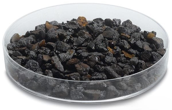
Germanium Monosulfide evaporation materials are typically supplied in forms such as granules, pieces, powders, or pellets optimized for thermal evaporation sources including resistive heating boats, crucibles, or electron-beam evaporation systems. High-purity GeS materials are carefully synthesized and refined to ensure consistent stoichiometry and minimal contamination during deposition.
During the evaporation process, GeS vaporizes under controlled vacuum conditions and condenses onto substrates to form thin films. The resulting films can be deposited on a variety of substrates including silicon, glass, sapphire, and flexible materials. Film properties such as crystallinity, morphology, and electrical characteristics can be tuned through deposition parameters such as substrate temperature and deposition rate.
Because GeS is considered a relatively environmentally benign semiconductor compared to many heavy-metal-based materials, it is receiving growing attention as a potential alternative material for sustainable optoelectronic technologies.
Applications
Germanium Monosulfide Evaporation Materials are primarily used in advanced semiconductor and optoelectronic research, including:
Thin film solar cells and photovoltaic absorber layers
Infrared and photodetection devices
Optoelectronic materials research involving IV–VI semiconductor compounds
Layered semiconductor thin films for next-generation electronics
Two-dimensional materials research based on layered chalcogenides
Semiconductor thin film fabrication for experimental electronic devices
These applications leverage the favorable electronic and optical characteristics of GeS thin films.
Technical Parameters
| Parameter | Typical Value / Range | Importance |
|---|---|---|
| Purity | 99.9% – 99.999% | High purity ensures reliable semiconductor performance |
| Composition | Stoichiometric GeS | Maintains consistent electronic properties |
| Form | Pieces / granules / powder / pellets | Compatible with various evaporation systems |
| Particle Size | 1 – 10 mm granules or customized | Suitable for evaporation sources |
| Melting Behavior | Sublimation under vacuum | Enables stable evaporation deposition |
| Deposition Method | Thermal evaporation / E-beam evaporation | Suitable for semiconductor thin film growth |
Comparison with Related Materials
| Material | Key Advantage | Typical Application |
|---|---|---|
| Germanium Monosulfide (GeS) | Layered semiconductor with suitable bandgap | Solar cells and optoelectronics |
| Germanium Selenide (GeSe) | Narrower bandgap for infrared devices | Photodetectors |
| Tin Sulfide (SnS) | Environmentally friendly photovoltaic absorber | Thin film solar cells |
| Germanium (Ge) | High carrier mobility | Semiconductor devices |
FAQ
| Question | Answer |
|---|---|
| What forms of Germanium Monosulfide evaporation materials are available? | GeS is typically supplied as granules, pellets, powders, or pieces suitable for thermal evaporation or electron-beam evaporation systems. |
| Can the material be customized? | Yes, purity level, particle size, and packaging can be customized according to deposition system requirements. |
| Which deposition methods are suitable for GeS? | Thermal evaporation and electron-beam evaporation are commonly used for depositing GeS thin films. |
| What substrates are compatible with GeS films? | Silicon, glass, sapphire, and other semiconductor or insulating substrates are commonly used. |
| Which industries use GeS evaporation materials? | Semiconductor research laboratories, photovoltaic development companies, optoelectronics research institutes, and advanced materials laboratories. |
Packaging
Our Germanium Monosulfide Evaporation Materials are meticulously tagged and labeled externally to ensure efficient identification and maintain high standards of quality control. We take great care to prevent any potential damage during storage and transportation, ensuring the materials arrive in perfect condition.
Conclusion
Germanium Monosulfide Evaporation Materials provide a reliable source for depositing high-quality semiconductor thin films with promising optical and electronic properties. Their layered structure, suitable bandgap, and environmentally friendly composition make GeS a valuable material for photovoltaic research, optoelectronic devices, and next-generation semiconductor technologies.
With customizable purity levels, particle sizes, and packaging options, GeS evaporation materials are well suited for a wide range of vacuum deposition systems.
For detailed specifications and a quotation, please contact us at sales@thinfilmmaterials.com.


Reviews
There are no reviews yet.