Introduction
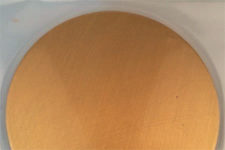
Gold Copper (Au/Cu) Sputtering Targets are alloy targets widely used in advanced thin film deposition processes for electronics, semiconductor devices, and precision coatings. By combining the excellent electrical conductivity and corrosion resistance of gold with the mechanical strength and cost efficiency of copper, Au/Cu alloy targets provide a balanced solution for producing durable conductive thin films.
In Physical Vapor Deposition (PVD) systems such as DC magnetron sputtering, Gold Copper sputtering targets enable the deposition of uniform alloy films with excellent adhesion, stable electrical performance, and improved structural durability. These thin films are widely applied in microelectronics, electronic contacts, bonding layers, and functional coatings where high conductivity and reliability are essential.
Detailed Description
Gold Copper Sputtering Targets are manufactured using high-purity gold and copper metals through advanced alloying techniques such as vacuum melting, casting, hot working, and precision machining. These processes ensure homogeneous alloy composition, high density, and a stable microstructure, which are essential for consistent sputtering performance and thin film quality.
Gold is known for its excellent electrical conductivity, chemical stability, and resistance to oxidation. Copper contributes additional mechanical strength and enhances adhesion to many substrates. When combined into an alloy sputtering target, these metals create thin films that maintain high electrical conductivity while improving mechanical durability compared to pure gold coatings.
The Au/Cu alloy composition can be customized to meet specific application requirements. Adjusting the ratio between gold and copper allows engineers to optimize electrical conductivity, film hardness, and material cost. This flexibility makes gold copper sputtering targets suitable for both research environments and industrial production.
Because the alloy is electrically conductive, DC magnetron sputtering is typically used for deposition. This method provides stable sputtering rates, high deposition efficiency, and uniform film thickness.
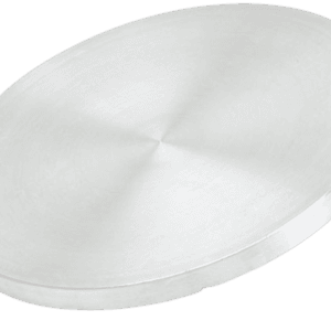
Gold Copper sputtering targets are available in circular discs, rectangular plates, and custom geometries compatible with most sputtering cathodes. For large-area deposition systems or high-power sputtering processes, the targets may be bonded to copper backing plates using indium bonding or elastomer bonding to enhance thermal conductivity and operational stability.
Applications
Thin films deposited from Gold Copper Sputtering Targets are used across a range of advanced technological applications:
Semiconductor devices – conductive layers and contact materials in integrated circuits.
Microelectronics manufacturing – thin films used in sensors, connectors, and electronic components.
Electrical contacts and connectors – corrosion-resistant conductive coatings.
Bonding and adhesion layers – intermediate layers in multilayer thin film structures.
Decorative coatings – durable metallic coatings with a gold-like appearance.
Research and development – alloy thin film studies in materials science laboratories.
Technical Parameters
| Parameter | Typical Value / Range | Importance |
|---|---|---|
| Purity | 99.9% – 99.99% metals | Higher purity improves film conductivity and device reliability |
| Composition | Custom Au/Cu ratios | Allows tuning of electrical and mechanical properties |
| Density | ≥99% theoretical | Ensures stable sputtering and uniform deposition |
| Diameter | 25 – 300 mm (custom) | Compatible with various sputtering cathodes |
| Thickness | 3 – 6 mm | Influences sputtering rate and target lifetime |
| Bonding | Copper backing plate (optional) | Improves heat transfer and structural stability |
Comparison with Related Materials
| Material | Key Advantage | Typical Application |
|---|---|---|
| Gold Copper (Au/Cu) | High conductivity with improved mechanical durability | Electronic contacts and conductive coatings |
| Pure Gold (Au) | Exceptional corrosion resistance and conductivity | Microelectronics and bonding layers |
| Copper (Cu) | Excellent electrical conductivity and low cost | Interconnects and conductive films |
FAQ
| Question | Answer |
|---|---|
| Can the Au/Cu sputtering target composition be customized? | Yes, the ratio of gold to copper can be tailored to meet specific electrical and mechanical performance requirements. |
| Which sputtering method is recommended for Au/Cu targets? | DC magnetron sputtering is typically used because the alloy is electrically conductive. |
| Are bonded targets available? | Yes, Au/Cu sputtering targets can be indium-bonded or elastomer-bonded to copper backing plates for improved thermal management. |
| What substrates are compatible with Au/Cu thin films? | Silicon wafers, glass, ceramics, and metal substrates are commonly used depending on the application. |
| Which industries commonly use Au/Cu sputtering targets? | Semiconductor manufacturing, microelectronics production, precision instrumentation, and materials science research. |
Packaging
Our Gold Copper Sputtering Targets are meticulously tagged and labeled externally to ensure efficient identification and maintain strict quality control standards. Each target is vacuum-sealed and carefully packed with protective cushioning materials to prevent contamination or mechanical damage during storage and transportation. Export-grade cartons or wooden crates are used for safe international delivery.
Conclusion
Gold Copper Sputtering Targets offer an ideal combination of electrical conductivity, corrosion resistance, and mechanical durability for advanced thin film deposition applications. By integrating the advantages of gold and copper, these alloy targets enable the production of reliable conductive coatings used in semiconductor devices, electronic components, and precision instruments.
With customizable compositions, high purity levels, and precision manufacturing, Au/Cu sputtering targets deliver consistent performance for both research laboratories and industrial thin film deposition systems.
For detailed specifications and a quotation, please contact us at sales@thinfilmmaterials.com.


Reviews
There are no reviews yet.