
Gold Sputtering Target Description

The gold sputtering target has the same properties as the precious metal gold (Au). Gold, symbolized as “Au,” originates from the Anglo-Saxon word “gold” and the Latin “aurum,” meaning “glow of sunrise.” It has been used since before 6000 BC, discovered by ancient Middle Eastern civilizations. Gold’s atomic number is 79, located in Period 6 and Group 11 of the periodic table, within the d-block. Its relative atomic mass is 196.966569(4) Dalton, with the number in brackets indicating uncertainty.
Gold is renowned for its beautiful yellow luster. It is soft, dense, malleable, ductile, and an excellent conductor of heat and electricity. Deposited films of gold sputtering targets and gold evaporation materials are used as layers in the production of semiconductors, sensors, batteries, and data storage.
Gold Sputtering Target Specification
| Material Type | Gold |
| Symbol | Au |
| Color/Appearance | Gold, Metallic |
| Melting Point | 1,064°C |
| Density | 19.3 g/cm3 |
| Sputter | DC |
| Type of Bond | Indium, Elastomer |
| Available Sizes | Dia.: 1.0″, 2.0″, 3.0″, 4.0″, 5.0″, 6.0″ Thick: 0.125″, 0.250″ |
We also offer other customized shapes and sizes of the sputtering targets; please Contact Us for more information.
Gold Sputtering Target Application
The gold sputtering target is used for standard scanning electron microscopy (SEM) coating, where it covers specimens with a thin conductive layer of gold. This prevents charging of specimens with an electron beam in conventional SEM mode and increases the signal-to-noise ratio.
Other applications include:
- Physical vapor deposition (PVD) of thin films
- Laser ablation deposition (PLD)
- Magnetron sputtering for semiconductors, displays, LEDs, and photovoltaic devices
Gold Sputtering Target Bonding Service
Specialized bonding services for Gold Sputtering Targets, including indium and elastomeric bonding techniques, enhance performance and durability. Thin Film Materials (TFM) ensures high-quality solutions that meet industry standards and customer needs.
We also offer custom machining of backing plates, which is essential for sputtering target assembly. This comprehensive approach improves target design flexibility and performance in thin film deposition. Our channels provide detailed information about bonding materials, methods, and services, helping clients make informed decisions.

Gold Sputtering Target Handling Notes
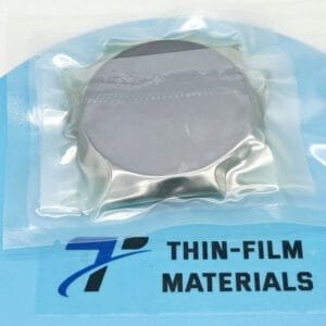
Gold Sputtering Target Packing
Our Gold Sputter Targets are clearly tagged and labeled externally to ensure efficient identification and quality control. We take great care to prevent any damage during storage and transportation.
Get Contact
TFM offers Gold Sputtering Targets in various forms, purities, sizes, and prices. We specialize in high-purity thin film deposition materials with optimal density and minimal grain sizes, which are ideal for semiconductor, CVD, and PVD applications in display and optics. Contact Us for current pricing on sputtering targets and other deposition materials that are not listed.


Reviews
There are no reviews yet.