Introduction
Indium Arsenide (InAs) Sputtering Target is a III–V compound semiconductor material well known for its narrow bandgap, high electron mobility, and strong infrared response. These properties make InAs thin films essential in infrared detectors, high-speed electronics, and optoelectronic devices. As a sputtering target, InAs enables controlled deposition of uniform semiconductor films with excellent electrical and optical performance for both research and advanced industrial applications.
Detailed Description
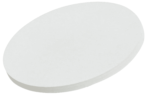
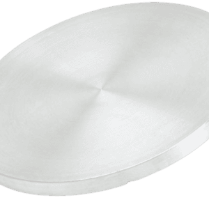
Our Indium Arsenide Sputtering Targets are fabricated from high-purity indium and arsenic sources using carefully controlled synthesis and consolidation processes. Strict control of stoichiometry is critical for InAs, as even small deviations in the In:As ratio can significantly influence carrier concentration, mobility, and crystalline quality of the deposited films.
The targets are produced with a dense, homogeneous microstructure to ensure stable sputtering behavior and minimal particle generation. InAs targets are typically used in RF sputtering systems due to their semiconducting nature, allowing precise control over deposition rate and film composition. Custom target sizes, thicknesses, and bonding options are available to match different sputtering tools and thermal management requirements.
Applications
Indium Arsenide Sputtering Targets are widely used in advanced semiconductor and optoelectronic thin film applications, including:
Infrared (IR) detectors and focal plane arrays
High-speed and low-noise electronic devices
Optoelectronic and photonic components
Narrow bandgap semiconductor research
Heterostructures and compound semiconductor devices
Academic and industrial R&D in III–V semiconductors
Technical Parameters
| Parameter | Typical Value / Range | Importance |
|---|---|---|
| Chemical Composition | InAs | Determines bandgap and carrier mobility |
| Purity | 99.9% – 99.99% | Reduces defect density in thin films |
| Diameter | 25 – 200 mm (custom available) | Compatible with standard sputtering systems |
| Thickness | 3 – 6 mm | Influences target lifetime and sputtering rate |
| Density | ≥ 95% theoretical | Improves plasma stability |
| Sputtering Mode | RF sputtering | Suitable for semiconducting compounds |
| Bonding | Unbonded / bonded on request | Enhances thermal stability |
Comparison with Related Materials
| Material | Key Advantage | Typical Application |
|---|---|---|
| InAs | Very high electron mobility, narrow bandgap | IR detectors & high-speed electronics |
| Indium Phosphide (InP) | Better thermal stability | Optoelectronics |
| Gallium Arsenide (GaAs) | Mature processing technology | RF & optoelectronic devices |
| Indium Antimonide (InSb) | Extremely narrow bandgap | Long-wavelength IR detection |
FAQ
| Question | Answer |
|---|---|
| Can the InAs sputtering target be customized? | Yes, diameter, thickness, purity, and bonding options can be tailored. |
| Is RF sputtering required for InAs? | RF sputtering is commonly used due to the semiconducting nature of InAs. |
| How is the target packaged? | Vacuum-sealed with protective cushioning and export-grade cartons or crates. |
| Is InAs suitable for infrared applications? | Yes, InAs is widely used for IR-sensitive thin film devices. |
Packaging
Our Indium Arsenide Sputtering Targets are meticulously tagged and externally labeled to ensure easy identification and strict quality control. Each target is vacuum-sealed and protected against moisture, oxidation, and mechanical damage during storage and transportation.
Conclusion
Indium Arsenide (InAs) Sputtering Target offers a reliable solution for depositing high-quality III–V semiconductor thin films with excellent electrical and infrared performance. With precise stoichiometric control, high purity, and flexible customization options, it is well suited for advanced semiconductor research and specialized device fabrication.
For detailed specifications and a quotation, please contact us at sales@thinfilmmaterials.com.


Reviews
There are no reviews yet.