
 MSDS File
Product Overview
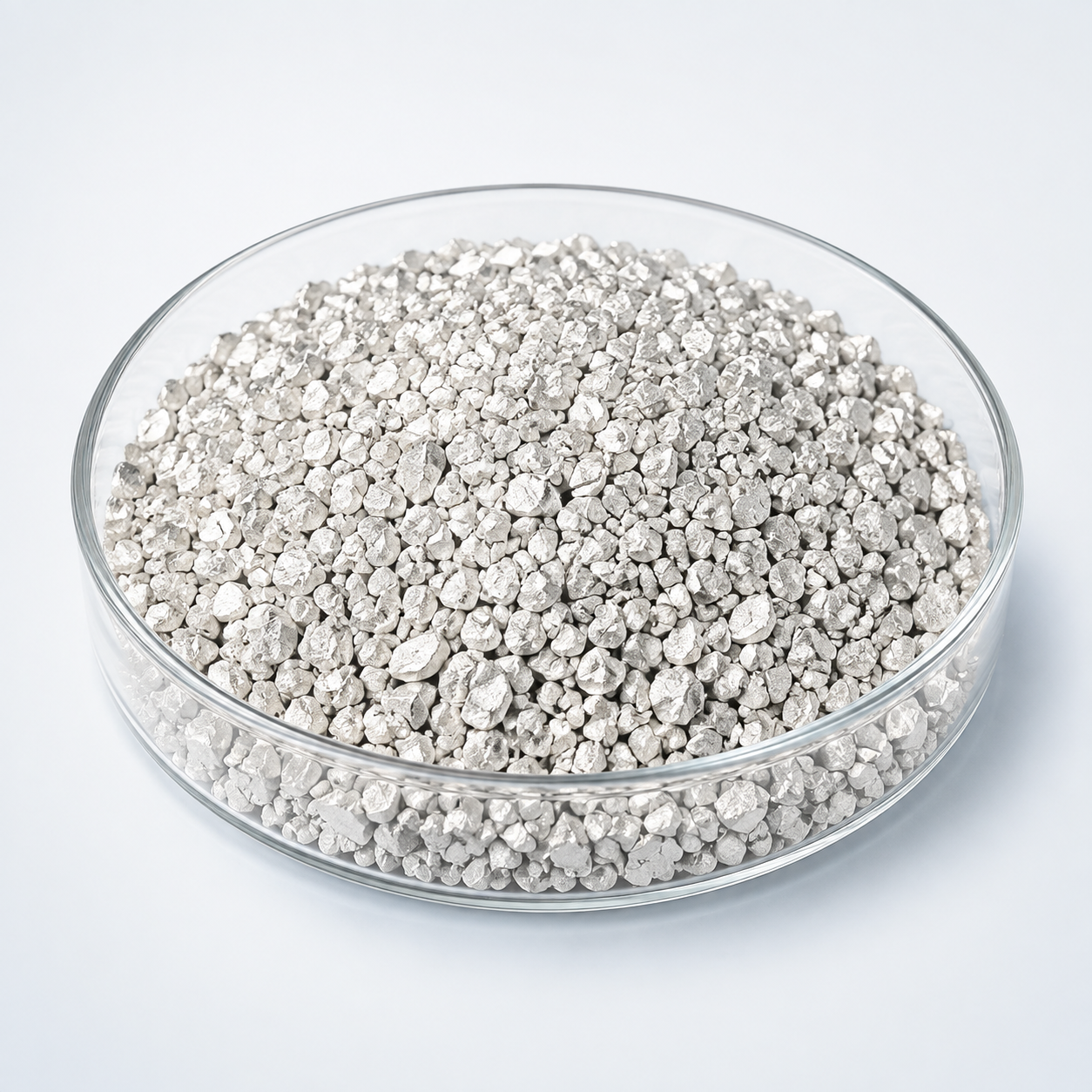
Indium Evaporation Materials (In) is an elemental evaporation material used to deposit metallic thin films by vacuum evaporation. Depending on vapor pressure, melting behavior, source geometry, and the available evaporator, the material may be processed by resistance heating, electron-beam evaporation, or another suitable high-vacuum source. For repeatable deposition, purity, source form, handling cleanliness, and compatibility with the boat, basket, crucible, or hearth are important procurement variables.
Evaporation Behavior and Process Considerations
The choice between resistance heating and electron-beam evaporation depends on vapor pressure, melting temperature, source mass, required rate, and the available boat or crucible. Low-to-moderate melting metals may be compatible with resistance heating, while higher-temperature materials can favor e-beam evaporation. Gradual preheating is useful for removing adsorbed gases and establishing a stable evaporation rate before deposition.
Technical Data
| Parameter | Typical Value / Range | Importance |
|---|---|---|
| Material | Indium (In) | Functional thin film source |
| Purity | 99.99% – 99.999% (4N–5N) | Reduces film impurities |
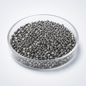
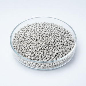
| Form | Pieces / Granules / Pellets | Compatible with evaporation systems |
| Melting Point | 156.6°C | Low thermal load deposition |
| Boiling Point | 2072°C | Suitable vapor pressure control |
| Deposition Method | E-beam / Thermal Evaporation | Flexible process options |
| Material | Key Advantage | Typical Application |
|---|---|---|
| Indium (In) | Low melting point & good conductivity | Conductive thin films |
| Indium Oxide | Transparent semiconductor | Display & photovoltaic coatings |
| ITO | High transparency + conductivity | Touch panels & displays |
| Gallium (Ga) | Semiconductor alloy component | Compound semiconductors |
| Question | Answer |
|---|---|
| Is indium suitable for thermal evaporation? | Yes, its low melting point makes it ideal for thermal evaporation systems. |
| Can ultra-high purity grades be supplied? | Yes, 4N to 5N purity levels are available for semiconductor applications. |
| Does indium oxidize easily? | A thin surface oxide may form in air, but this does not significantly affect evaporation performance. |
| Can customized shapes be provided? | Yes, material form can be tailored to specific crucible or source requirements. |
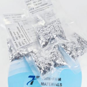
| How is it packaged? | Vacuum-sealed packaging prevents contamination and moisture exposure during shipment. |
Typical Thin-Film Applications
- Indium metallic coatings for electronic, optical, conductive, reflective, catalytic, or contact-layer applications
- Semiconductor and laboratory PVD research
- Multilayer stacks and co-evaporation processes requiring a pure elemental source
Source Form and Ordering Considerations
For quotation, provide material, purity, source form, particle or piece size, quantity, evaporation method, and any boat, basket, crucible, or e-beam hearth constraints. If the material will be used for a specific coating stack, sharing the intended film thickness or deposition application can help with source-form selection and packaging recommendations.
Frequently Asked Questions
Can Indium be used for thermal evaporation?
It depends on melting point, vapor pressure, charge size, and the source hardware. Many elemental metals can be resistance-heated, while higher-temperature materials are often more convenient to evaporate with an electron beam.
How do I choose between pellets, pieces, and granules for Indium?
Choose a form that loads securely into the boat, crucible, basket, or e-beam pocket and provides stable heating. Smaller pieces can improve packing, while larger pieces may reduce handling and dust.
Why should Indium be preheated before opening the shutter?
Preheating removes adsorbed gases and stabilizes the evaporation flux. This can reduce pressure spikes, spitting, and contamination during the actual film deposition.
Can the crucible material affect Indium evaporation?
Yes. At elevated temperature, the charge can react with, dissolve, wet, or contaminate some source materials. Crucible and boat compatibility should be checked for the actual evaporation temperature.
Does source purity directly affect film purity?
Source purity is one of the main contributors to film contamination, although chamber cleanliness, crucible condition, substrate preparation, and background pressure also affect the final film.
What information should I send TFM for Indium evaporation material?
Please provide purity, preferred source form and size, quantity, evaporation method, source-holder details, and any packaging, inspection, or documentation requirements.
Reviews
There are no reviews yet.