Generic selectors
Exact matches only
Search in title
Search in content
Post Type Selectors

ST0021 Indium Sputtering Target, In

Chemical Formula: In
Catalog Number: ST0021
CAS Number: 7440-74-6
Purity: 99.99%, 99.999%
Shape: Discs, Plates, Column Targets, Step Targets, Custom-made

Indium sputtering target  come in various forms, purities, sizes, and prices. Thin Film Materials (TFM) manufactures and supplies top-quality sputtering targets at competitive prices.

MSDS File

Availability: 1 in stock

Indium Sputtering Target Description

Indium

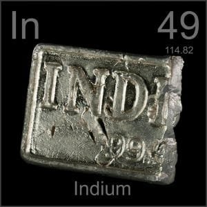
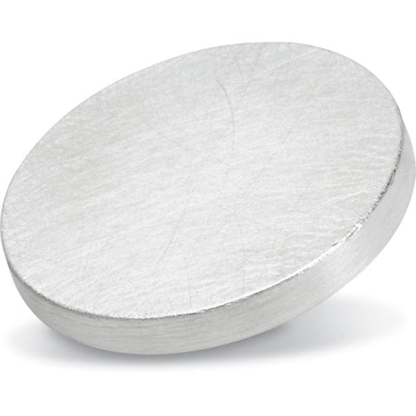
The indium sputtering target is a silvery, lustrous gray target made from high-purity indium metal. Indium, symbolized as “In,” derives its name from the Latin word ‘indicium,’ meaning violet or indigo. First mentioned in 1863 by F. Reich and T. Richter, who later isolated it, indium has an atomic number of 49, located in Period 5, Group 13 of the periodic table, within the p-block. Its relative atomic mass is 114.818(3) Dalton, with the number in brackets indicating uncertainty.

Indium compounds are evaporated under vacuum to form thin films used in electronics and photovoltaic cells. Pure indium is also used as a film layer in semiconductors.

Indium Sputtering Target Specification

Material Type Indium
Symbol In
Color/Appearance Silvery Lustrous Gray, Metallic
Melting Point 157 °C
Type of Bond Elastomer
Density 7.3 g/cc
Thermal Conductivity 82 W/m.K
Coefficient of Thermal Expansion 32.1 x 10⁻⁶/K
Comments Wets W and Cu. Use Mo liner. Low Melting Point materials not ideal for sputtering.
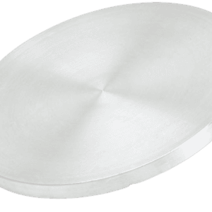
Available Sizes Dia.: 1.0″, 2.0″, 3.0″, 4.0″, 5.0″, 6.0″
Thick: 0.125″, 0.250″

We also offer other customized shapes and sizes of the sputtering targets; please Contact Us for more information.

Indium Sputtering Target Applications

The indium sputtering target is used to coat bearings of high-speed motors, ensuring the even distribution of lubricating oil. Indium targets are also employed for thin film deposition, decoration, semiconductors, displays, LEDs, photovoltaic devices, functional coatings, optical information storage, glass coatings (such as car and architectural glass), and optical communication.

Additionally, indium is used in the production of electrical components like rectifiers, thermistors, and photoconductors. It is also utilized to make mirrors that are as reflective as silver mirrors but more resistant to tarnishing. Indium is used in low melting alloys, with a notable alloy consisting of 24% indium and 76% gallium, which remains liquid at room temperature.

Indium Sputtering Target Target Bonding

Specialized bonding services for Indium Sputtering Targets, including indium and elastomeric bonding techniques, enhance performance and durability. Thin Film Materials (TFM) ensures high-quality solutions that meet industry standards and customer needs.

We also offer custom machining of backing plates, which is essential for sputtering target assembly. This comprehensive approach improves target design flexibility and performance in thin film deposition. Our channels provide detailed information about bonding materials, methods, and services, helping clients make informed decisions.

Packaging

Our Indium Sputtering Targets are clearly tagged and labeled externally to ensure efficient identification and quality control. We take great care to prevent any damage during storage and transportation.

Get Contact

TFM offers Indium Sputtering Targets in various forms, purities, sizes, and prices. We specialize in high-purity thin film deposition materials with optimal density and minimal grain sizes, which are ideal for semiconductor, CVD, and PVD applications in display and optics. Contact Us for current pricing on sputtering targets and other deposition materials that are not listed.

Reviews

There are no reviews yet.

Be the first to review “ST0021 Indium Sputtering Target, In”

Your email address will not be published. Required fields are marked *

Related Products

FAQ

It’s the source material (in solid form) used in sputter deposition to eject atoms or molecules that then form a thin film on a substrate.

Targets can be pure metals (e.g., gold, copper, aluminum), ceramics (e.g., Al₂O₃, SiO₂, TiO₂), alloys, or composites—chosen based on the film’s desired properties.


They are produced by processes such as melting/casting for metals or sintering (often with hot isostatic pressing) for ceramics and composite targets to ensure high density and purity.


In a vacuum chamber, a plasma (typically argon) bombards the target, ejecting atoms that travel and condense on a substrate, forming a thin film.


Key factors include the target’s purity, density, grain structure, and the sputtering yield (i.e. how many atoms are ejected per incident ion), as well as operating conditions like power density and gas pressure.


Operators monitor target erosion (often by measuring the depth of the eroded “race track”) or track total energy delivered (kilowatt-hours) until it reaches a threshold that can compromise film quality.


Fragile materials (such as many ceramics or certain oxides) and precious metals often require a backing plate to improve cooling, mechanical stability, and to allow thinner targets that reduce material costs.


DC sputtering is used for conductive targets, while RF sputtering is necessary for insulating targets (like many oxides) because it prevents charge buildup on the target’s surface.


In reactive sputtering, a reactive gas (e.g., oxygen or nitrogen) is introduced to form compound films on the substrate, but it may also “poison” the target surface if not carefully controlled.


Many manufacturers prefer to control raw material quality by sourcing their own powders; using external powders can risk impurities and inconsistent target properties.


Targets should be stored in clean, dry conditions (often in original packaging or re-wrapped in protective materials) and handled with gloves to avoid contamination, ensuring optimal performance during deposition.

Deposition rate depends on factors such as target material and composition, power density, working gas pressure, substrate distance, and the configuration of the sputtering system (e.g., magnetron design).

 
Shopping Cart
Scroll to Top