 MSDS File
Introduction
Indium(III) Telluride (In₂Te₃) Evaporation Materials are widely used in vacuum thin-film deposition for semiconductor, optoelectronic, and phase-change related applications. As a III–VI compound semiconductor, In₂Te₃ offers tunable electrical and optical properties, making it an important source material for research and industrial coating processes that require precise film composition and high material purity.
Detailed Description
Our Indium(III) Telluride Evaporation Materials are manufactured from high-purity indium and tellurium through carefully controlled synthesis and consolidation processes to ensure accurate stoichiometry and chemical homogeneity. Strict control of composition is essential for In₂Te₃, as deviations can directly influence film conductivity, optical absorption, and phase behavior.
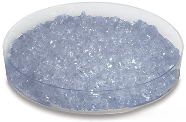
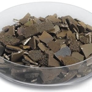
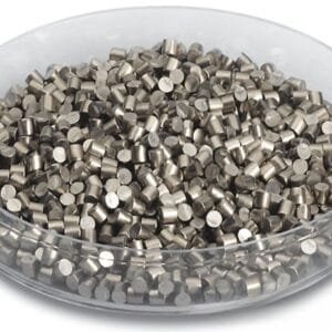
The material is supplied in forms suitable for thermal evaporation and electron-beam evaporation, such as pellets, pieces, or granules. Optimized particle size and density promote stable evaporation rates and minimize spitting or compositional drift during deposition. High purity levels help reduce oxygen and metallic contaminants, resulting in smoother films with reproducible electrical and optical characteristics.
In₂Te₃ evaporation materials are compatible with high-vacuum and ultra-high-vacuum systems and can be used in single-source evaporation or co-evaporation processes, depending on film design requirements. Custom sizing and packaging options are available to match specific crucibles, boats, or evaporation sources.
Applications
Indium(III) Telluride Evaporation Materials are commonly used in:
Semiconductor and compound semiconductor thin films
Phase-change memory (PCM) research and development
Infrared and optoelectronic devices
Thermoelectric and chalcogenide-based materials research
Thin-film laboratories and academic R&D
They are particularly valuable in applications requiring precise control of film stoichiometry and reproducible material performance.
Technical Parameters
| Parameter | Typical Value / Range | Importance |
|---|---|---|
| Chemical Formula | In₂Te₃ | Defines compound semiconductor properties |
| Purity | 99.99% – 99.999% | Reduces impurities affecting film performance |
| Form | Pellets / Pieces / Granules | Compatible with various evaporation sources |
| Deposition Method | Thermal / E-beam evaporation | Supports different vacuum processes |
| Vacuum Compatibility | HV / UHV | Ensures low contamination and stable deposition |
| Packaging | Vacuum-sealed | Prevents oxidation and moisture absorption |
Comparison with Related Materials
| Material | Key Advantage | Typical Application |
|---|---|---|
| Indium(III) Telluride (In₂Te₃) | Tunable electrical & optical properties | Phase-change & semiconductor films |
| Indium Telluride (InTe) | Different stoichiometry | Specialized semiconductor research |
| Germanium Telluride (GeTe) | Strong phase-change behavior | PCM devices |
FAQ
| Question | Answer |
|---|---|
| Can the material form be customized? | Yes, pellets, chunks, or granules can be supplied based on your evaporation setup. |
| Is it suitable for e-beam evaporation? | Yes, In₂Te₃ is commonly used in e-beam evaporation systems. |
| How is purity controlled? | High-purity raw materials and controlled synthesis ensure accurate stoichiometry. |
| Do you provide small R&D quantities? | Yes, small and bulk quantities are both available. |
Packaging
Our Indium(III) Telluride Evaporation Materials are vacuum-sealed, clearly labeled, and packaged with protective materials to maintain purity and prevent contamination during storage and transportation.
Conclusion
Indium(III) Telluride (In₂Te₃) Evaporation Materials provide a reliable and high-purity solution for depositing advanced chalcogenide and semiconductor thin films. With controlled stoichiometry, flexible material forms, and compatibility with standard vacuum evaporation techniques, they are well suited for both research and industrial applications.
For detailed specifications and a quotation, please contact us at sales@thinfilmmaterials.com.

Reviews
There are no reviews yet.