 MSDS File
Introduction
Indium Tin Oxide (ITO) Evaporation Material is a high-performance compound used for depositing transparent and conductive thin films in advanced optoelectronic, display, and photovoltaic systems. ITO combines optical transparency with electrical conductivity, making it a cornerstone material for modern electronic interfaces and optically active surfaces.
Related Products: Indium Evaporation Materials, Tin Evaporation Materials
Detailed Description
Indium tin oxide is a mixed oxide consisting primarily of indium oxide (In₂O₃) doped with tin oxide (SnO₂). It behaves as a wide bandgap, n-type semiconductor with excellent transmission in the visible range and useful electrical conductivity.
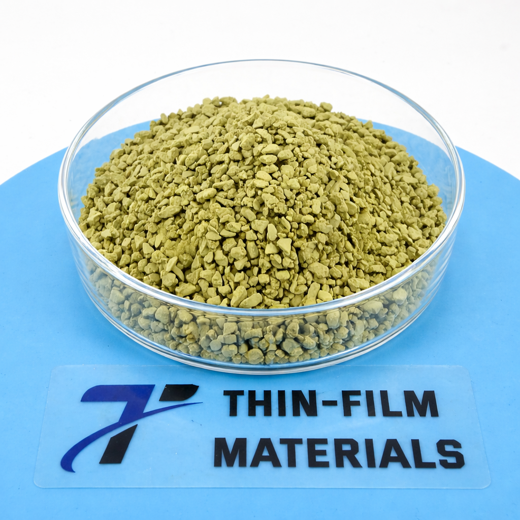
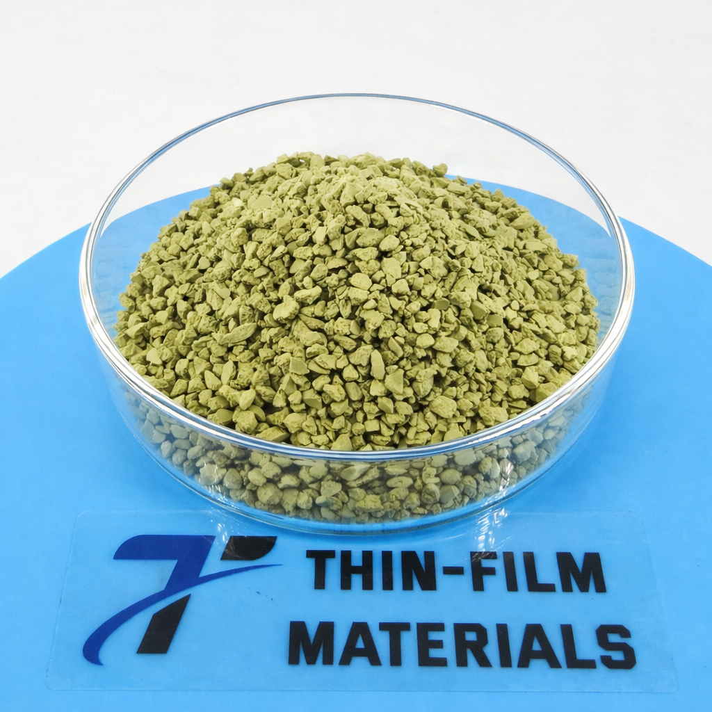
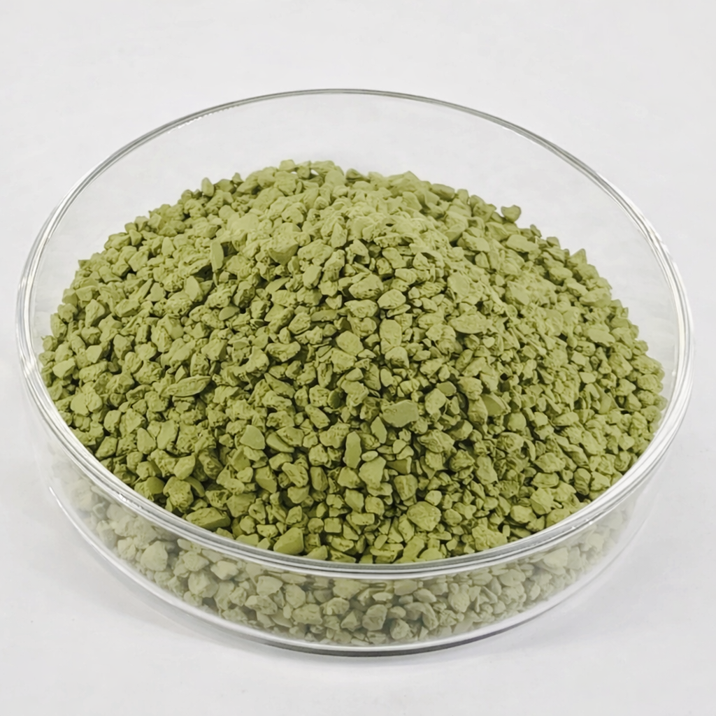
ITO evaporation materials are typically supplied as high-purity pellets, granules, or pieces, engineered for thermal or electron-beam evaporation in vacuum deposition systems. The controlled composition and microstructure support stable evaporation behavior and consistent transfer of material to the growing film.
Key performance features include:
Optical transparency: Thin films can transmit over 80% of visible light, ideal for transparent electrodes.
Electrical conductivity: Effective for transparent conductive coatings in electronic devices.
Chemical stability: Resists degradation and corrosion under typical operating conditions.
ITO evaporation materials are available with customizable purity and form factors to match specific crucible or evaporation source requirements.
Applications
Indium Tin Oxide evaporation material is widely used in:
Transparent conductive films for displays and touch panels
Photovoltaic electrodes and smart window coatings
Optoelectronic and sensor device fabrication
Anti-static and EMI shielding thin films
Advanced surface coatings requiring light transmission with conductivity
Technical Parameters
| Parameter | Typical Value / Range | Importance |
|---|---|---|
| Composition | In₂O₃ / SnO₂ mixed oxide | Defines conductive and optical properties |
| Purity | 99.9% – 99.99% | Reduces contamination, improves film quality |
| Form | Pellets / Pieces / Custom | Matches vacuum evaporation equipment |
| Melting Range | ~1500-1900 °C (depends on composition) | Suitable for high-temperature vacuum sources |
| Density | ~7.1-7.2 g/cm³ | Reference for deposition calibration |
Comparison with Related Materials
| Material | Key Advantage | Typical Application |
|---|---|---|
| ITO Evaporation Material | Excellent transparency + conductivity | Transparent electrodes |
| AZO (Al-doped ZnO) | Lower cost, better environmental stability | Alternative TCO for photovoltaics |
| FTO (Fluorine-doped SnO₂) | Good thermal stability | High-temperature TCO needs |
ITO remains the most established transparent conducting oxide for high-performance thin films, especially where combined optical and electrical function is required.
FAQ
| Question | Answer |
|---|---|
| Can ITO evaporation materials be custom shaped? | Yes, sizes and forms can be tailored to specific deposition systems. |
| What deposition methods are supported? | Thermal and electron-beam evaporation are common, though sputtering is often preferred for uniform films. |
| How does ITO film performance vary? | Optical transparency and conductivity depend on film thickness, oxygen content, and deposition parameters. |
| Is post-deposition treatment required? | Annealing in controlled atmospheres is frequently used to optimize film conductivity and transparency. |
Packaging
Our Indium Tin Oxide Evaporation Materials are clearly labeled and packed using protective methods to minimize oxidation and contamination. Vacuum sealing or inert gas packing is used to preserve material integrity during storage and international transportation.
Conclusion
Indium Tin Oxide (ITO) Evaporation Material delivers dependable performance for depositing high-quality transparent, conductive films across a wide range of electronic and optoelectronic applications. With customizable forms and high purity, it supports both cutting-edge research and industrial coating needs.
For detailed specifications and a quotation, please contact us at sales@thinfilmmaterials.com.
Ordering Table
| Material | Size | Quantity | Purity | Part Number |
| Indium Tin Oxide | 1/8" - 1/4" Pieces | 1 lb. | 99.99% | EVMITO40 |
| Indium Tin Oxide | 1/8" - 1/4" Pieces | 25 g | 99.99% | EVMITO40A |
| Indium Tin Oxide | 1/8" - 1/4" Pieces | 50 g | 99.99% | EVMITO40B |
| Indium Tin Oxide | 1/8" - 1/4" Pieces | 100 g | 99.99% | EVMITO40D |
| Indium Tin Oxide | 1/8" - 1/4" Pieces | 250 g | 99.99% | EVMITO40J |
| Indium Tin Oxide | 1/8" - 1/4" Pieces | 1 kg | 99.99% | EVMITO40KG |
| Indium Tin Oxide | 1/8" - 1/4" Pieces | 500 g | 99.99% | EVMITO40T |


Reviews
There are no reviews yet.