
Indium Tin Sputtering Target Description
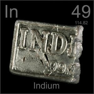 Indium is a chemical element derived from the Latin word ‘indicium,’ which refers to the violet or indigo color seen in its spectral lines. It was first discovered in 1863 by F. Reich and T. Richter, with its isolation confirmed and announced by T. Richter. The symbol for indium is “In,” and it is positioned in Period 5, Group 13 of the periodic table, within the p-block. Its atomic number is 49, and its relative atomic mass is 114.818(3) Dalton, with the number in brackets reflecting the associated uncertainty.
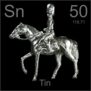
Tin, known as *stannum* in Latin, comes from the Anglo-Saxon word “tin,” which means “hard.” This element has been utilized since around 3500 BC. Represented by the symbol “Sn,” tin is located in Period 5, Group 14 of the periodic table, within the p-block. It has an atomic number of 50 and a relative atomic mass of 118.710(7) Dalton, with the number in brackets indicating the associated uncertainty.
Related Products: Indium Sputtering Target, Tin Sputtering Target.
Indium Tin Sputtering Target Specifications
| Material Type | Indium Tin |
| Symbol | In/Sn |
| Color/Appearance | Metallic solid in various forms including powder, sputtering target, foil, bar, plate |
| Melting Point | 117 °C |
| Density | / |
| Available Sizes | Dia.: 2.0″, 3.0″, 4.0″, 5.0″, 6.0″ Thick: 0.125″, 0.250″ |
We also offer other customized shapes and sizes of the sputtering targets; please Contact Us for more information.
Indium Tin Sputtering Target Application
The Indium Tin Sputtering Target is utilized in various applications, including thin film deposition, decorative coatings, and in the production of semiconductors. It is particularly effective for use in displays, LEDs, and photovoltaic devices. Additionally, it serves in functional coatings and is valuable for optical information storage, glass coatings for both automotive and architectural purposes, and optical communication technologies.
Packing
Our Indium Tin Sputtering Targets are meticulously tagged and labeled to facilitate easy identification and ensure rigorous quality control. We take extensive measures to prevent any potential damage during both storage and transportation, ensuring the targets arrive in pristine condition.
Related products
-
ST0013 Erbium Sputtering Target, Er
$355.00 – $520.00 -
ST0001 Aluminum Sputtering Target, Al
$79.20 – $142.60


Reviews
There are no reviews yet.